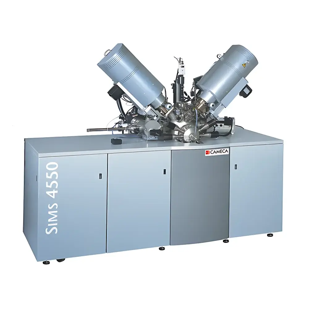
CAMECA QUAD4550 Secondary Ion Mass Spectrometer
| Brand | Cameca |
|---|---|
| Origin | France |
| Model | QUAD4550 |
| Instrument Type | Quadrupole SIMS |
| Primary Ion Beam Energy Range | 250 eV – 5 keV |
| Mass Range | 1–350 Da |
| Mass Resolution | Not Available |
| Base Pressure | ≤1×10⁻¹⁰ mbar (≤1×10⁻⁸ Pa) |
Overview
The CAMECA QUAD4550 is a high-performance quadrupole-based Secondary Ion Mass Spectrometer (SIMS) engineered for quantitative depth profiling and ultra-trace elemental analysis of advanced semiconductor materials. Operating on the principle of dynamic SIMS, the instrument sputters the sample surface with a focused primary ion beam (O₂⁺ or Cs⁺), generating secondary ions that are mass-analyzed by a high-transmission quadrupole mass filter. Its design prioritizes depth resolution down to sub-nanometer scales—critical for characterizing dopant distributions in sub-10 nm transistor gates, interfacial layers in high-k/metal gate stacks, SiGe heterostructures, and III–V compound semiconductors (e.g., GaN, InP). The system achieves exceptional sensitivity for light elements—including H, C, N, and O—enabled by an ultra-high vacuum (UHV) environment (<1×10⁻¹⁰ mbar) and low-noise ion detection architecture. Unlike magnetic sector or time-of-flight SIMS platforms, the QUAD4550 delivers rapid, reproducible quantification across wide dynamic ranges without sacrificing analytical throughput—making it particularly suited for process development, failure analysis, and routine QC in semiconductor R&D and fab environments.
Key Features
- Quadrupole mass analyzer optimized for high transmission and stable mass calibration over extended acquisition periods
- Primary ion column supporting dual-source operation (O₂⁺ and Cs⁺) with continuous energy tuning from 250 eV to 5 keV—enabling controlled sputter yield and minimized atomic mixing for shallow-depth profiling
- UHV main chamber backed by turbomolecular and ion pumps, maintaining base pressure ≤1×10⁻¹⁰ mbar to suppress background interferences and enhance signal-to-noise ratio for light-element detection
- Dedicated charge compensation system integrating both electron flood gun and UV laser options for reliable analysis of insulating films (e.g., SiO₂, HfO₂, Al₂O₃)
- Motorized sample stage accommodating substrates from small chips (≥3 mm × 3 mm) up to full 100 mm wafers, with precise XYZ positioning and tilt capability for angle-resolved sputtering
- Stabilized ion optics and electronics delivering measurement repeatability with RSD < 0.2% for repeated depth profiles under identical conditions
Sample Compatibility & Compliance
The QUAD4550 supports direct analysis of conductive and non-conductive solid samples without metallization or matrix enhancement. It is routinely deployed for metrology of epitaxial layers, gate oxides, diffusion barriers, and 2D material heterostructures. The platform complies with standard semiconductor industry measurement protocols aligned with ASTM E1597 (Standard Guide for SIMS Analysis), ISO/IEC 17025 requirements for testing laboratories, and supports audit-ready data handling per FDA 21 CFR Part 11 when integrated with validated software configurations. All vacuum subsystems meet CE and RoHS directives; electrical safety conforms to IEC 61010-1.
Software & Data Management
Acquisition and evaluation are performed using CAMECA’s proprietary SIMS Suite software, which provides intuitive workflow management, real-time spectral visualization, and automated depth-scale calibration via reference standards (e.g., NIST SRM 2137). Each measurement session logs complete instrument parameter sets—including beam energy, current, dwell time, aperture configuration, and vacuum status—into a relational database. This ensures full traceability and enables one-click re-execution of prior analyses. Export formats include ASCII, CSV, and HDF5 for interoperability with third-party modeling tools (e.g., TCAD simulators). Optional modules support GLP/GMP-compliant electronic signatures, audit trails, and role-based user access control.
Applications
- Ultra-shallow junction profiling of B, P, As in Si and SiGe channels
- Quantitative oxygen and carbon contamination mapping at Si/SiO₂ interfaces
- Depth-resolved stoichiometry verification of ALD-grown high-k dielectrics (HfO₂, ZrO₂, LaAlO₃)
- Interdiffusion analysis in III–V heterojunctions (e.g., InGaAs/InP, GaN/AlGaN)
- Hydrogen distribution measurement in passivated silicon surfaces and amorphous SiNₓ films
- Thin-film uniformity assessment across 100 mm wafers with automated stage rastering
FAQ
What is the typical depth resolution achievable with the QUAD4550 for boron in silicon?
Under optimized low-energy O₂⁺ sputtering (≤500 eV) and cryogenic sample cooling, depth resolution of ≤0.8 nm can be achieved for B in Si near the surface (0–5 nm), consistent with published SIMS inter-laboratory benchmarks.
Can the QUAD4550 perform isotopic ratio measurements?
Yes—the quadrupole mass filter enables stable peak centering and reproducible integration for isotopic pairs such as ²⁸Si/²⁹Si or ¹⁶O/¹⁸O, though its mass resolving power limits separation of isobaric interferences (e.g., ¹⁴N⁺ vs. ¹⁴C⁺) without energy filtering.
Is remote operation supported?
Fully supported via secure VNC or TLS-encrypted client-server architecture; all acquisition, alignment, and reporting functions are accessible from off-site locations with appropriate network permissions.
How is calibration traceability maintained?
Instrument response is calibrated using certified reference materials (CRMs) traceable to NIST or PTB, with periodic verification against in-house standards monitored through long-term drift studies logged in the central database.
Related Products