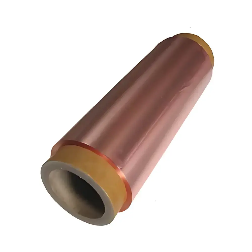
Copper Foil for Graphene Synthesis
| Brand | KJ GROUP (Shenyang Kejing) |
|---|---|
| Origin | Liaoning, China |
| Manufacturer Type | Authorized Distributor |
| Country of Origin | China |
| Model | Cu Foil (Graphene-Grade) |
| Thickness | 25 µm |
| Dimensions | 150 mm × 150 mm |
| Electrical Conductivity | 97% IACS @ 20 °C |
| Particle Size (Surface Roughness Ra) | 0.02 mm |
| Density | 8.94 g/cm³ |
| Vickers Hardness | 80 HV |
| Tensile Strength (Longitudinal) | 28 kgf/mm² |
| Elongation | 3–8% min |
| Resistivity | ≤0.017165 Ω·mm/m |
| Net Weight | 5 kg |
Overview
This high-purity, graphene-grade copper foil is engineered specifically for chemical vapor deposition (CVD) synthesis of large-area, continuous monolayer and few-layer graphene films. Fabricated from electrolytic tough pitch (ETP) copper with controlled grain structure and ultra-low surface roughness, the foil delivers exceptional thermal stability, uniform nucleation density, and minimal defect propagation during high-temperature annealing (up to 1050 °C in H2/CH4/Ar atmospheres). Its precisely defined 25 µm thickness ensures optimal thermal mass distribution and mechanical handling integrity during roll-to-roll or batch CVD processes, while maintaining sufficient ductility for transfer-compatible substrate preparation.
Key Features
- Optimized surface morphology: Average surface roughness (Ra) ≤ 0.02 mm — critical for uniform graphene domain growth and reduced grain boundary formation
- High electrical purity: 97% International Annealed Copper Standard (IACS) conductivity at 20 °C, indicating low residual oxygen and impurity content (<50 ppm total metallic impurities)
- Controlled metallurgical structure: Fine-grained, recrystallized microstructure with preferred (111) crystallographic orientation enhances graphene epitaxy
- Dimensional stability: Tensile strength of 28 kgf/mm² (≈275 MPa) and elongation of 3–8% ensure resistance to warping and cracking during thermal cycling
- Low resistivity: ≤0.017165 Ω·mm/m — consistent with ASTM B170-21 specifications for high-conductivity copper foils
- Traceable manufacturing: Batch-certified material with documented heat treatment history, surface passivation status, and cleanliness verification (ISO 14644 Class 8 cleanroom handling)
Sample Compatibility & Compliance
The foil is compatible with standard CVD reactors (cold-wall and hot-wall configurations), electrochemical delamination setups, and polymer-assisted wet transfer protocols (e.g., PMMA or PDMS stamping). It meets baseline requirements for ISO/IEC 17025-accredited laboratories performing graphene process development. While not certified to specific regulatory frameworks (e.g., FDA or USP), its documented purity profile, absence of halogenated contaminants, and compliance with RoHS Directive 2011/65/EU make it suitable for academic, industrial R&D, and pre-GMP pilot-scale graphene production environments. Material Safety Data Sheet (MSDS) and Certificate of Analysis (CoA) are available upon request for each production lot.
Software & Data Management
No embedded firmware or proprietary software is associated with this passive substrate material. However, KJ GROUP provides digital documentation support including downloadable CoA templates, recommended CVD parameter guidelines (temperature ramp rates, gas flow ratios, dwell times), and cross-referenced literature citations (e.g., aligned with protocols published in Nature Materials and ACS Nano). All technical data files are timestamped, version-controlled, and archived per internal quality management system (QMS) aligned with ISO 9001:2015 clause 7.5. For traceability, each foil sheet is labeled with a unique batch ID linked to furnace log records and surface profilometry reports.
Applications
- CVD growth of monolayer and bilayer graphene on catalytic Cu substrates
- Template-assisted synthesis of graphene nanoribbons and patterned domains via masked etching
- Reference substrate for Raman mapping calibration (G/2D peak intensity ratio, FWHM analysis)
- Electrode base layer in flexible transparent conductors and hybrid heterostructures
- Substrate for transfer-free device fabrication using direct dielectric encapsulation
- Calibration standard for scanning electron microscopy (SEM) and atomic force microscopy (AFM) resolution testing
FAQ
Is this copper foil oxygen-free (OFHC)?
No — it is electrolytic tough pitch (ETP) copper (C11000), containing ~200–400 ppm oxygen. This level supports controlled oxide formation during annealing, which aids graphene domain alignment without compromising conductivity.
Can the foil be reused after graphene transfer?
Not recommended. Surface contamination, carbon residue, and microstructural changes after high-temperature exposure reduce nucleation repeatability. Single-use protocol is advised for reproducible monolayer yield.
What cleaning protocol do you recommend prior to CVD?
Standard sequence: acetone ultrasonication (10 min), isopropanol rinse, DI water wash, N2 blow-dry, followed by in-situ H2 annealing at 1000 °C for 30 min under 100 sccm flow.
Do you supply custom dimensions or thicknesses?
Yes — KJ GROUP offers OEM cutting and rolling services; minimum order quantity applies. Custom thicknesses (12–50 µm) and widths up to 300 mm are available with lead time confirmation.
How is surface roughness verified?
Each production lot undergoes non-contact white-light interferometry (WLI) per ISO 25178-2, with 5-point sampling across the sheet and full report included in the CoA.


