E+H Metrology MX 204 Semi-Automatic Wafer Thickness & Geometry Metrology System
| Brand | E+H Metrology |
|---|---|
| Origin | Germany |
| Manufacturer Type | Authorized Distributor |
| Origin Category | Imported |
| Model | MX 204 |
| Pricing | Available Upon Request |
| Wafer Diameter | 100 mm, 125 mm, 150 mm, 200 mm, 300 mm |
| Thickness Accuracy | ±0.5 µm to ±1.0 µm |
| Thickness Resolution | 75 nm to 1.0 µm |
| Thickness Range | 100–1000 µm |
| Measurement Principle | Dual-Sided Capacitive Sensing |
| Measured Parameters | Thickness, Total Thickness Variation (TTV), Bow, Warp, Surface Flatness, Stress-Induced Deformation |
Overview
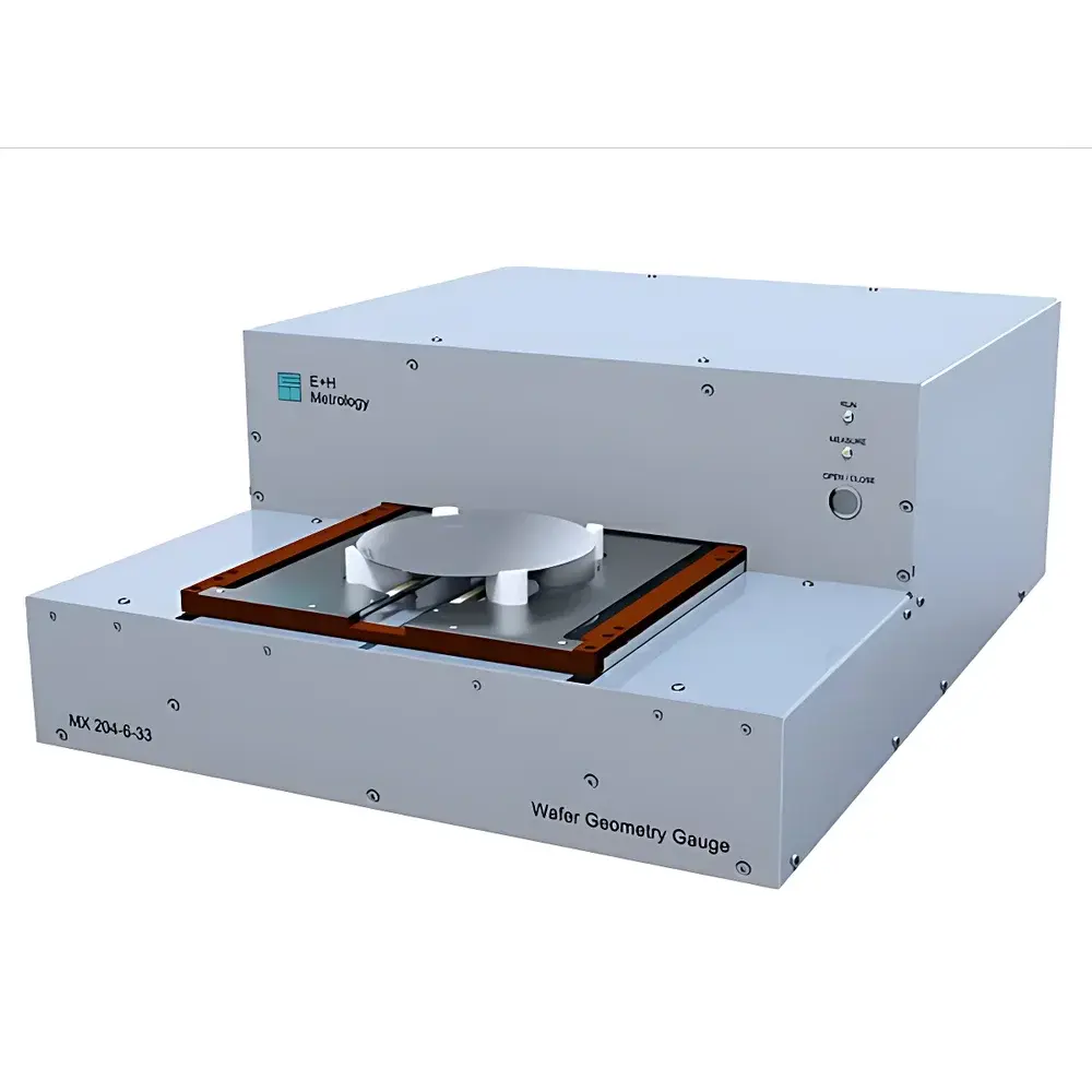
The E+H Metrology MX 204 is a precision semi-automatic metrology system engineered for non-contact, high-resolution geometric characterization of semiconductor wafers. It employs dual-sided capacitive sensing technology—where matched electrode pairs are positioned above and below the wafer—to simultaneously acquire distance measurements from both surfaces relative to fixed reference planes. This architecture enables direct, traceable determination of absolute thickness, surface separation, and spatial deviation across the full wafer area. Unlike optical interferometric or eddy-current methods, capacitive metrology offers exceptional stability against ambient temperature fluctuations, minimal sensitivity to surface reflectivity or coating variations, and immunity to vibration-induced phase noise—making it especially suitable for cleanroom-integrated process control environments. The MX 204 is designed for use in front-end semiconductor manufacturing, R&D laboratories, and advanced packaging facilities where quantitative, repeatable assessment of mechanical integrity and planarization performance is required prior to lithography, CMP, or bonding steps.
Key Features
- Dual-axis capacitive sensor array with calibrated electrode pairs enabling simultaneous top- and bottom-surface distance acquisition
- Semi-automatic operation with programmable Z-axis stage positioning and manual wafer loading via ergonomic chuck interface
- Support for standard wafer diameters: 100 mm (4″), 125 mm (5″), 150 mm (6″), 200 mm (8″), and 300 mm (12″) with optional carrier adapters
- Thickness accuracy certified to ±0.5 µm (typ.) over 100–1000 µm range; resolution down to 75 nm per measurement point
- Integrated thermal drift compensation algorithm using real-time sensor head temperature monitoring
- Modular firmware architecture supporting configurable scan patterns (grid, radial, edge-dense) and user-defined ROI selection
- Robust mechanical design compliant with SEMI S2/S8 safety standards and ISO 14644-1 Class 5 cleanroom compatibility
Sample Compatibility & Compliance
The MX 204 accommodates bare and coated wafers fabricated from silicon (Si), silicon carbide (SiC), gallium nitride (GaN), gallium arsenide (GaAs), and indium phosphide (InP). Its capacitive measurement principle remains insensitive to native oxide layers, thin dielectric films (<5 µm), or conductive metallization—enabling reliable metrology across diverse process stacks without recalibration. All measurement algorithms adhere to ASTM F397 (Standard Test Method for Total Thickness Variation of Silicon Wafers) and SEMI MF-1530 (Specification for Wafer Geometry Measurement Systems). Raw data files include embedded metadata conforming to ASTM E1392 (Standard Practice for Data Exchange Between Semiconductor Equipment and Host Systems), facilitating integration into factory-wide MES/SPC platforms.
Software & Data Management
The system operates under E+H’s proprietary WaferMetro™ v4.x software suite, which provides full GLP-compliant audit trail functionality—including operator ID logging, parameter change history, calibration event timestamps, and electronic signature support aligned with FDA 21 CFR Part 11 requirements. Measurement reports export natively in CSV, XML, and industry-standard SECS/GEM-compliant HSMS format. Advanced analysis modules include TTV contour mapping, bow/warp decomposition via Zernike polynomial fitting (up to 36 terms), and stress calculation using Stoney’s equation with user-input material constants (Young’s modulus, Poisson’s ratio). Data archiving supports networked storage with role-based access control and automated backup scheduling.
Applications
- Pre- and post-CMP thickness uniformity verification for Si and wide-bandgap substrates
- Process qualification of epitaxial growth, SOI layer transfer, and wafer bonding operations
- Stress profiling in strained-Si, SiGe heterostructures, and GaN-on-Si templates
- Failure analysis of warpage-related delamination in fan-out wafer-level packaging (FOWLP)
- Calibration reference for inline ellipsometers and interferometric film-thickness tools
- Qualification of reclaimed wafers and substrate reuse protocols in pilot-line environments
FAQ
Does the MX 204 require vacuum or inert gas purging during operation?
No. The capacitive sensors operate reliably in ambient cleanroom air; no environmental enclosure is needed.
Can the system measure patterned or structured wafers (e.g., MEMS devices or trench-etched substrates)?
Yes—provided feature depth does not exceed 5 µm and surface roughness remains below Ra < 10 nm; local capacitance perturbations are mitigated via adaptive averaging.
Is NIST-traceable calibration documentation provided with each unit?
Yes. Each MX 204 ships with a factory calibration certificate traceable to PTB (Physikalisch-Technische Bundesanstalt) standards, including uncertainty budgets per ISO/IEC 17025.
What maintenance intervals are recommended for long-term accuracy retention?
Annual verification of sensor linearity and stage repeatability is advised; no consumables or periodic sensor replacement is required.
How is edge exclusion defined during TTV computation?
Default edge exclusion is 2 mm from wafer perimeter, configurable between 0.5–5.0 mm in software to align with customer-specific metrology SOPs.


