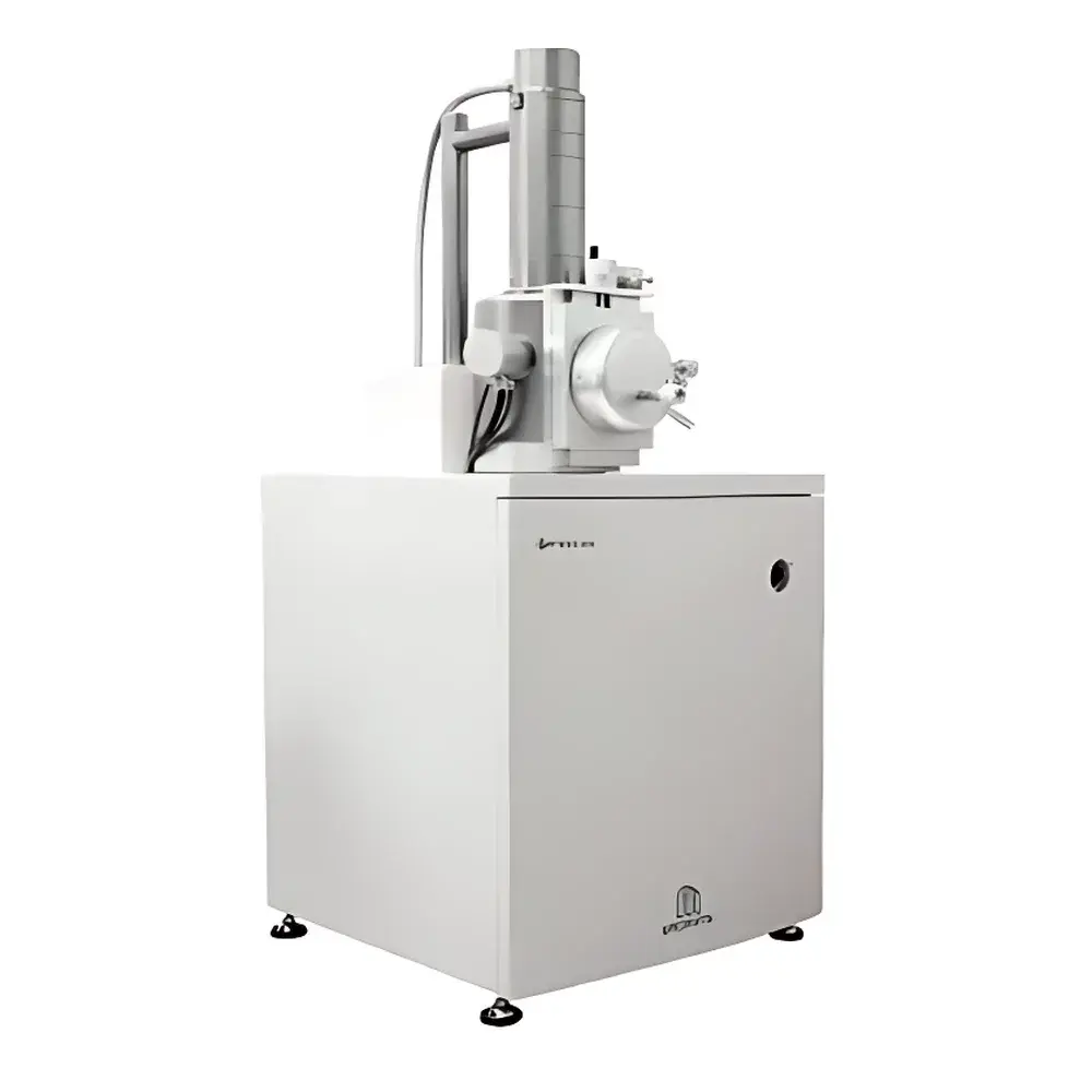
EMCrafts CUBE-1000/1100 Desktop Scanning Electron Microscope
| Brand | EMCrafts |
|---|---|
| Origin | South Korea |
| Model | CUBE-1000/1100 |
| Instrument Type | Desktop SEM |
| Electron Source | Tungsten Filament |
| Pumping Time | 90 s (evacuation), 10 s (vent) |
| Gun Alignment | Auto-aligned, no manual adjustment required |
| Form Factor | Benchtop, footprint < 0.5 m² |
Overview
The EMCrafts CUBE-1000/1100 is a fully integrated desktop scanning electron microscope engineered for rapid deployment and routine high-resolution imaging in resource-constrained or multi-user laboratory environments. Unlike conventional floor-standing SEMs requiring dedicated rooms, vibration isolation tables, and extended pump-down cycles, the CUBE series employs a compact, sealed-column architecture with a thermally stable tungsten hairpin filament electron source and differential pumping stages optimized for fast vacuum cycling—achieving operational readiness in under 90 seconds after chamber venting. Its operation relies on standard secondary electron (SE) detection, with optional backscattered electron (BSE) capability available on the CUBE-1100 configuration. The system operates at accelerating voltages ranging from 1 kV to 20 kV, enabling surface-sensitive low-voltage imaging and deeper material interaction at higher energies—making it suitable for both conductive and lightly coated non-conductive specimens without mandatory metal sputtering in many cases.
Key Features
- Sub-10 nm resolution at 20 kV (verified per ISO 16700 Annex B using gold-on-carbon test samples)
- Benchtop footprint (< 480 × 430 × 420 mm) with integrated vacuum system, eliminating external turbomolecular pumps and chillers
- Automated vacuum sequence: full evacuation in ≤90 seconds; chamber venting completed in ≤10 seconds—enabling >20 sample changes per hour
- Self-aligning tungsten filament source with >1,500-hour nominal lifetime and no user-accessible gun alignment procedures
- Integrated digital scan generator and real-time image acquisition at up to 1,024 × 768 pixels with 16-bit depth and line-scan averaging
- Onboard EDS interface support (via USB 3.0) for third-party energy-dispersive X-ray spectrometers compliant with ASTM E1508 and ISO 22309
Sample Compatibility & Compliance
The CUBE-1000/1100 accommodates standard 32 mm diameter stub-mounted specimens up to 40 mm in height and 50 mm in diameter. Optional motorized stage variants support X-Y-Z translation with ±25 mm travel and tilt (±45°) for cross-sectional viewing. Specimen chambers are compatible with carbon tape, silver paint, and colloidal graphite conductive media. The system meets IEC 61000-6-3 (EMC emission) and IEC 61000-6-2 (immunity) standards. All firmware and control software comply with FDA 21 CFR Part 11 requirements for electronic records and signatures when operated with audit-trail-enabled acquisition modules—supporting GLP/GMP workflows in QC laboratories across pharmaceutical, materials, and electronics sectors.
Software & Data Management
Control and acquisition are managed via EMCrafts’ proprietary SEMSuite™ v4.x software, running on embedded Windows 10 IoT Enterprise. The interface provides intuitive workflow-driven operation: auto-focus, auto-stigmation, brightness/contrast optimization, and stage navigation via touchscreen or mouse. Image metadata—including kV, probe current, dwell time, magnification, working distance, and detector mode—is embedded in TIFF and BMP exports using EXIF-compatible tags. Raw image buffers support batch export in HDF5 format for downstream quantitative analysis in MATLAB, Python (SciPy/NumPy), or commercial platforms such as ImageJ/Fiji. Software update history, user login logs, and parameter change timestamps are retained for ≥18 months to satisfy internal audit and regulatory review requirements.
Applications
The CUBE platform serves as a primary characterization tool across academic, industrial, and service-laboratory settings. In materials science, it supports morphology assessment of sintered ceramics, fracture surface analysis of alloys per ASTM E3, particle size distribution of catalyst powders (ISO 13322-1), and coating uniformity verification in thermal barrier systems. In life sciences, it enables high-contrast imaging of freeze-dried biological tissues, pollen grain ultrastructure, and drug carrier microspheres without heavy-metal staining. Within semiconductor manufacturing, it facilitates quick failure analysis of bond pads, solder joint integrity checks, and lithography residue inspection on wafers up to 200 mm diameter. Geological applications include mineral phase identification in thin sections and porosity quantification in shale cores per API RP 40 protocols.
FAQ
Does the CUBE-1000/1100 require liquid nitrogen or external cooling?
No. The tungsten filament and detector electronics are air-cooled; no cryogenic support is needed.
Can non-conductive samples be imaged without sputter coating?
Yes—low-kV imaging (1–3 kV) combined with charge compensation via beam deceleration enables direct observation of polymers, ceramics, and biological specimens in many cases.
Is remote operation supported?
Yes. SEMSuite™ includes VNC-compatible remote desktop functionality with role-based access control and TLS 1.2 encrypted session handshaking.
What maintenance intervals are recommended?
Filament replacement every 1,500 hours; vacuum pump oil change every 6 months or 2,000 operating hours; annual calibration verification using certified NIST-traceable resolution standards.
How is data integrity ensured during long acquisitions?
All acquisitions write directly to redundant internal SSDs with journaling file system (NTFS); power-loss recovery preserves partial frames and metadata up to the last committed buffer.