Femto-NSOM Series 249 Advanced Near-Field Scanning Optical Microscope
| Origin | Canada |
|---|---|
| Supplier Type | Authorized Distributor |
| Origin Category | Imported Instrument |
| Model | 249 |
| Pricing | Available Upon Request |
| Scan Range (Measurement Head) | 80 × 80 × 3.5 µm (±10%) |
| Minimum Step Size | 0.009 nm |
| XY Sample Stage Travel | 5 × 5 mm |
| Stage Positioning Accuracy | 5 µm |
| Maximum Sample Diameter/Thickness | Φ100 × 10 mm |
| Closed-Loop XY Piezo Platform Range | 100 × 100 µm |
| Inherent Nonlinearity | <0.2% |
| Positional Accuracy | 2 nm |
| Repeatability | 30 nm (typical), <0.2% of full scale |
| Maximum Load Capacity | 2 kg |
| Laser Pulse Duration | <50 fs |
| Average Output Power | >100 mW |
| Repetition Rate | >80 MHz |
| Tunable Wavelength Range | 740–950 nm |
| Optional Laser Modules | Trestles 20/50/100 (700–950 nm), Mavericks65 (1240–1270 nm), Tamarak-Er (1540–1560 nm) |
Overview
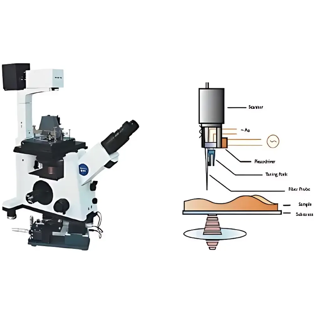
The Femto-NSOM Series 249 is a high-resolution, fiber-coupled near-field scanning optical microscope engineered for nanoscale optical characterization with ultrafast temporal resolution. It operates on the principle of aperture-type scanning near-field optical microscopy (SNOM/NSOM), where sub-diffraction-limit spatial resolution is achieved by local illumination and detection through a metal-coated tapered optical fiber probe with an effective aperture diameter below 100 nm. Unlike conventional far-field microscopy constrained by the Abbe diffraction limit (~λ/2), this system delivers optical imaging resolution down to ~50 nm—enabling direct visualization of plasmonic hotspots, quantum emitter localization, photonic crystal bandgap features, and nanoscale heterogeneity in 2D materials. The integration of femtosecond pulsed excitation enables time-resolved pump-probe NSOM measurements, supporting ultrafast carrier dynamics mapping in semiconductors, exciton diffusion studies in perovskites, and coherent phonon imaging in nanostructured dielectrics.
Key Features
- Tangential-force feedback mechanism ensures stable, non-contact probe-sample interaction while maintaining sub-nanometer topographic registration during optical acquisition.
- Multi-modal operation: configurable reflection-mode, fluorescence-mode, and transmission-mode NSOM—compatible with both opaque and transparent substrates including Si/SiO₂ wafers, glass coverslips, and freestanding membranes.
- Femtosecond laser excitation (80 MHz repetition rate, tunable 740–950 nm) provides high peak intensity for nonlinear optical contrast (e.g., two-photon fluorescence, second-harmonic generation) without thermal damage to delicate biological or organic samples.
- Closed-loop piezoelectric XY stage (100 × 100 µm range, 2 nm accuracy, <0.2% inherent nonlinearity) guarantees quantitative positional fidelity across extended scan areas and multi-region correlation experiments.
- Modular laser architecture supports optional wavelength extension modules—including Trestles (700–950 nm), Mavericks65 (1240–1270 nm), and Tamarak-Er (1540–1560 nm)—enabling resonance-matched excitation of telecom-band emitters, Er³⁺-doped waveguides, or mid-IR vibrational probes.
Sample Compatibility & Compliance
The Femto-NSOM Series 249 accommodates standard microscope-compatible samples up to Φ100 mm in diameter and 10 mm in thickness, including silicon wafers, ITO-coated glass, polymer thin films, exfoliated TMDCs, and cultured neuronal networks on glass-bottom dishes. All mechanical and optical components comply with ISO 10110-7 (surface quality of optical elements) and ISO 14644-1 Class 5 cleanroom handling requirements for probe assembly. The instrument’s control firmware and data acquisition architecture are designed to support GLP-compliant workflows, including audit-trail logging, user-access level management, and timestamped metadata embedding per image frame—facilitating traceability in regulated R&D environments aligned with FDA 21 CFR Part 11 principles.
Software & Data Management
Control and analysis are performed via proprietary FemtoScan Suite v4.x—a platform-independent application built on Qt/C++ with Python API extensions. The software supports synchronized acquisition of topography (via shear-force feedback), optical intensity (PMT signal), polarization-resolved channels, and optional spectral data from integrated CCD spectrometers. Raw datasets are stored in HDF5 format with embedded calibration parameters (e.g., probe transmission efficiency, laser power stability logs, piezo voltage-to-displacement coefficients). Batch processing pipelines include drift correction, deconvolution-based resolution enhancement, and cross-correlation alignment for multimodal overlay (e.g., NSOM + AFM topography + confocal fluorescence). Export options include TIFF (16-bit), CSV (pixel-by-pixel spectral traces), and MRC (for EM-style structural reconstruction interoperability).
Applications
- Nanoscale photoluminescence mapping of quantum dots, hBN defects, and WSe₂ monolayers under resonant femtosecond excitation.
- In situ monitoring of plasmon-enhanced photocatalysis on Au nanorod arrays with simultaneous topographic feedback.
- Sub-100 nm resolution infrared absorption contrast imaging using wavelength-tunable Er-fiber laser excitation (1540–1560 nm) coupled with lock-in detection.
- Time-resolved carrier diffusion profiling in perovskite solar cell absorbers via pump-probe NSOM with <100 fs temporal gating.
- Correlative optical-electrical nanoscopy: integration with conductive AFM modules for concurrent photocurrent mapping and local density of states analysis.
FAQ
What is the minimum resolvable feature size under optimal conditions?
Under ambient conditions with a calibrated Al-coated fiber probe (aperture ~70 nm) and 800 nm excitation, lateral resolution is typically 50–60 nm, verified using NIST-traceable line-width standards (SRM 2053).
Is vacuum or cryogenic operation supported?
The base system operates in air or nitrogen-purged enclosures; optional vacuum-compatible stages and low-temperature sample holders (4–300 K) are available as OEM-integrated modules.
Can the system be upgraded for tip-enhanced Raman spectroscopy (TERS)?
Yes—the optical path and XYZ nanopositioning architecture are fully compatible with TERS configurations; gold-coated AFM probes with plasmonic tips can be mounted using the standard cantilever holder.
How is laser power stability maintained during long-duration scans?
An integrated photodiode-based active power stabilization loop maintains output fluctuation below ±0.5% RMS over 8-hour acquisitions, with real-time logging of incident power at the probe input.
Does the software support automated region-of-interest (ROI) stitching?
Yes—tile-based mosaic acquisition with sub-pixel overlap correction and seam-free blending is implemented using fiducial marker tracking or cross-correlation algorithms.


