Filmetrics R50 Four-Point Probe Sheet Resistance Tester
| Brand | KLA |
|---|---|
| Origin | USA |
| Manufacturer Type | Authorized Distributor |
| Product Origin | Imported |
| Model | Filmetrics R50 |
| Automation Level | Manual |
| Sheet Resistance Range | 1 mΩ/□ – 200 MΩ/□ |
| Sheet Resistance Accuracy | ±1% |
| Substrate Size Compatibility | 4-inch to 12-inch wafers |
| Software | RSMapper™ |
| Probe Compatibility | Fully compatible with KLA’s full suite of four-point probe sensors |
| XY Stage | 200 mm motorized |
| Z-Travel | 100 mm precision-controlled |
| Measurement Configurations | Customizable grid, linear, radial, and user-defined point patterns |
| Application Scope | Conductive & semiconducting thin films on Si, GaAs, SiC, sapphire, glass, and flexible substrates |
Overview
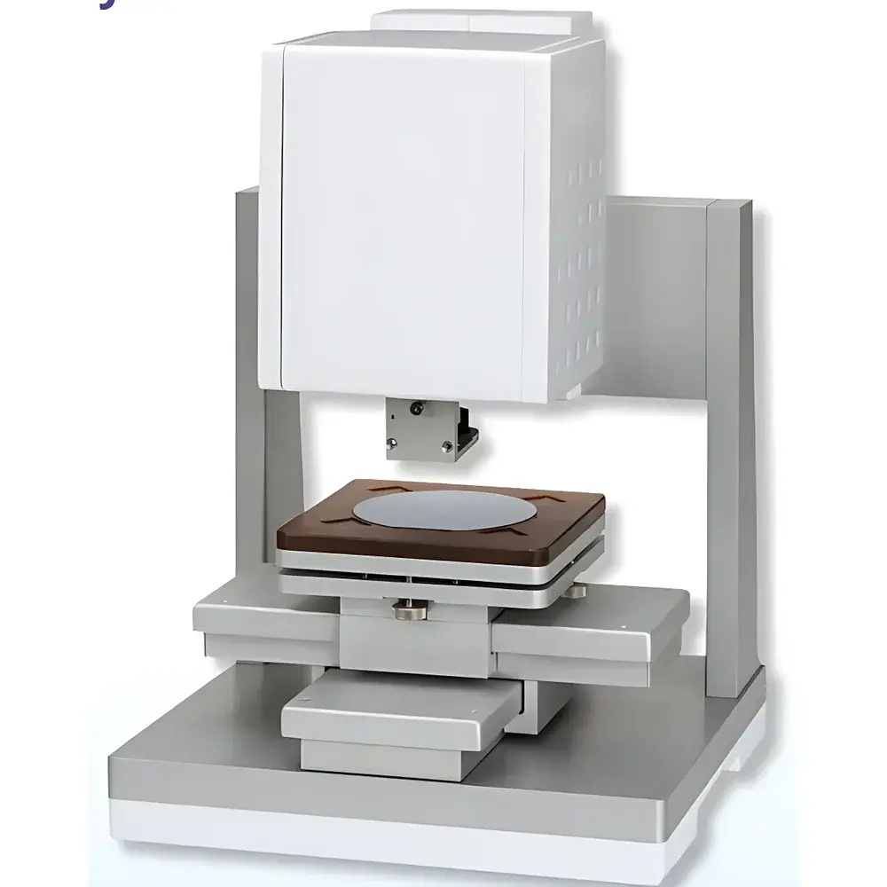
The Filmetrics R50 Four-Point Probe Sheet Resistance Tester is an engineered metrology platform developed by Filmetrics — a KLA company — for high-fidelity, non-destructive sheet resistance (Rs) characterization of conductive and semiconducting thin films. Operating on the established four-point probe (4PP) principle, the system eliminates voltage drop errors inherent in two-point measurements by separating current injection and voltage sensing functions across four collinear, equally spaced tungsten carbide probes. Complementing this contact-based modality, the R50 integrates optional eddy-current (EC) non-contact measurement capability for rapid, wear-free mapping of conductive layers — particularly valuable for delicate or patterned surfaces where probe contact may induce damage or contamination. Designed explicitly for semiconductor process development and quality control, the R50 delivers traceable, reproducible Rs data across ten decades (1 mΩ/□ to 200 MΩ/□), supporting process monitoring from heavily doped silicon to ultra-thin transparent conductive oxides (TCOs) and 2D materials.
Key Features
- Dual-mode operation: Simultaneous support for standardized four-point probe (ASTM F84, ISO 10474) and non-contact eddy-current (EC) measurement — enabling method selection based on film integrity requirements and process stage.
- Precision mechanical architecture: 200 mm × 200 mm motorized XY stage with sub-micron repeatability and 100 mm programmable Z-axis travel, ensuring stable probe landing force control and consistent tip-to-surface engagement.
- Wide dynamic range: Validated Rs measurement coverage from 1 mΩ/□ (highly conductive metal films) to 200 MΩ/□ (lightly doped semiconductors or resistive oxides), with ±1% accuracy referenced to NIST-traceable standards.
- Flexible spatial sampling: User-defined measurement layouts — including rectangular grids, linear scans, polar coordinate sweeps, and arbitrary point lists — facilitate targeted defect analysis, edge profiling, and wafer-level uniformity assessment.
- Probe interoperability: Native compatibility with KLA’s family of calibrated four-point probes (e.g., CDE, KLA-Tencor legacy probes), allowing seamless integration into existing metrology workflows and cross-platform data correlation.
- Robust stage calibration: Built-in auto-calibration routines for XY positioning and Z-force feedback ensure long-term measurement stability under varying environmental conditions and repeated use cycles.
Sample Compatibility & Compliance
The R50 accommodates bare and patterned wafers from 100 mm (4-inch) to 300 mm (12-inch) diameter, including silicon, compound semiconductors (GaAs, InP, SiC), sapphire, fused silica, and flexible polymer substrates. It supports both front-side and back-side probing configurations, with vacuum chuck options available for thin or warped substrates. All electrical measurements comply with ASTM F84 (Standard Test Method for Measuring Resistivity of Silicon Wafers Using Four-Point Probes) and ISO 10474 (Semiconductor materials — Specification of silicon wafers). The system architecture supports GLP/GMP-aligned operation through audit-trail-enabled software logging and user-access controls — facilitating alignment with FDA 21 CFR Part 11 requirements when integrated into regulated manufacturing environments.
Software & Data Management
RSMapper™ software provides a unified interface for instrument control, real-time data visualization, statistical process monitoring (SPC), and report generation. It enables automated recipe-driven measurements, spatial heatmapping of Rs distribution, and overlay with CAD layer files for correlation with lithographic features. Raw measurement data is stored in vendor-neutral CSV and HDF5 formats, supporting downstream analysis in MATLAB, Python (NumPy/Pandas), or JMP. Version-controlled software updates and configurable export templates ensure compatibility with enterprise MES and SPC systems. Optional API access allows integration into factory automation frameworks (SECS/GEM, OPC UA).
Applications
- Semiconductor front-end process control: Ion implant dose verification, anneal uniformity mapping, and epitaxial layer resistivity grading.
- Compound semiconductor fabrication: Characterization of AlGaN/GaN HEMT channel layers, dopant activation efficiency in InP-based photonic devices.
- Advanced packaging: Cu pillar and redistribution layer (RDL) sheet resistance uniformity assessment pre- and post-bonding.
- Display technologies: ITO, AZO, and graphene-based transparent electrode homogeneity evaluation on TFT-LCD, OLED, and microLED substrates.
- Photovoltaics: Thin-film solar cell emitter sheet resistance profiling and passivation layer optimization.
- Flexible electronics: Conductive ink and printed metal trace resistance validation on PET, PI, and paper substrates.
FAQ
Does the R50 require recalibration between different substrate sizes?
No — the motorized stage and probe alignment system are designed for automatic compensation across 4-inch to 12-inch wafers; only initial mechanical zeroing is required per setup.
Can the R50 measure through dielectric capping layers?
Contact 4PP mode requires direct metallic or semiconducting surface access; however, the optional eddy-current module can characterize underlying conductive layers beneath thin, non-conductive dielectrics (e.g., <1 µm SiO₂ or SiNx).
Is RSMapper compliant with FDA 21 CFR Part 11 for electronic records?
Yes — when deployed with role-based user authentication, electronic signatures, and immutable audit trails enabled, RSMapper meets core Part 11 requirements for regulated environments.
What probe force ranges are supported?
Standard probe loading is adjustable from 0.5 g to 10 g per tip, with closed-loop Z-force feedback ensuring consistent contact pressure regardless of substrate warpage or surface topography.
How is measurement traceability maintained?
Each R50 system ships with a KLA-certified calibration certificate traceable to NIST Standard Reference Materials (SRMs), and includes onboard reference resistor arrays for daily performance verification.


