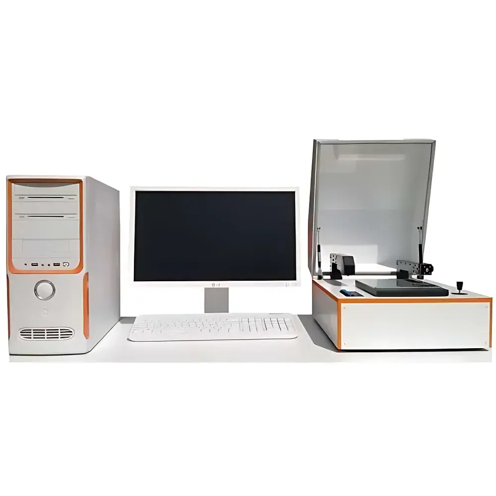
FPP Scan Four-Point Probe Sheet Resistance Mapping System
| Brand | pv-tools |
|---|---|
| Origin | Germany |
| Model | 4ppscan |
| Automation Level | Semi-Automatic |
| Max Test Current | 30 mA |
| Mapping Area | 10 × 10 cm |
| Measurement Duration (10×10 grid) | 4 min |
| Probe Tip Radius | 0.25 mm |
| Weight | 16 kg |
| Dimensions (L×W×H) | 36 × 48 × 24 cm |
| Vacuum Chuck Material | Borosilicate Glass |
| Probe Material | Tungsten Carbide |
| Software Features | Color-mapped resistivity visualization, histogram analysis, line-scan extraction, point re-measurement, I–V sweep linearity validation, auto-numbering |
Overview
The FPP Scan Four-Point Probe Sheet Resistance Mapping System is a precision-engineered semiconductor metrology instrument designed for non-destructive, high-spatial-resolution characterization of sheet resistance (Rs) and lateral resistivity uniformity across planar substrates. Based on the established four-point probe (4PP) principle—where two outer probes inject current and two inner probes measure voltage drop—the system eliminates contact resistance errors and delivers traceable, quantitative Rs values in ohms per square (Ω/□). Engineered for photovoltaic (PV) process development and quality control, the FPP Scan operates under ambient or low-vacuum conditions using a borosilicate glass vacuum chuck, enabling stable, particle-free sample immobilization without mechanical clamping-induced stress or surface damage. Its semi-automatic architecture integrates mechanical scanning with real-time software control, supporting repeatable, operator-independent mapping of large-area wafers, thin-film solar cells, transparent conductive oxides (TCOs), and doped silicon layers.
Key Features
- Semi-automated XY stage with programmable 10 × 10 cm mapping area and sub-millimeter positional repeatability
- Interchangeable tungsten carbide probe heads with certified 0.25 mm tip radius, recognized by system firmware for automatic calibration factor application
- Borosilicate glass vacuum chuck with integrated pneumatic seal—designed for rapid cleaning, chemical resistance, and minimal thermal drift
- Auto-initiation protocol: measurement sequence starts immediately upon lid closure, minimizing ambient contamination and operator variability
- Real-time I–V sweep capability with linearity validation (R² ≥ 0.9998 typical) to confirm ohmic contact behavior and detect localized non-uniformities
- Integrated current sourcing up to 30 mA with programmable polarity reversal to mitigate thermoelectric offset and electrode polarization effects
Sample Compatibility & Compliance
The FPP Scan accommodates rigid flat substrates up to 150 mm × 150 mm and thicknesses from 100 µm to 3 mm—including monocrystalline and multicrystalline silicon wafers, CIGS and perovskite absorber stacks, ITO and FTO-coated glass, and laser-doped selective emitters. All probe-contact surfaces meet ISO 14644-1 Class 5 cleanroom compatibility requirements when operated in controlled environments. The system supports ASTM F84-22 (Standard Test Method for Measuring Resistivity of Silicon Wafers) and aligns with IEC 60404-13 for magnetic materials characterization where applicable. Data acquisition and storage comply with GLP audit-trail requirements via timestamped metadata embedding (operator ID, date/time, probe ID, environmental conditions).
Software & Data Management
The proprietary pv-tools Control Suite provides full instrument orchestration and post-processing capabilities. Users generate customizable color-mapped Rs distributions with selectable palettes (jet, viridis, grayscale), overlay contour lines, and export georeferenced TIFF or CSV files. Histograms quantify spatial distribution statistics (mean, σ, min/max), while interactive line scans extract cross-sectional profiles along arbitrary axes. A single-click “re-measure” function allows targeted re-acquisition at any pixel without full-map repetition. All I–V sweeps are stored with raw voltage/current arrays, enabling offline verification of Ohm’s law compliance. Exported datasets conform to HDF5 format for interoperability with MATLAB, Python (NumPy/Pandas), and JMP statistical platforms.
Applications
- Process qualification of diffusion, ion implantation, and annealing steps in Si PV cell fabrication
- Uniformity assessment of sputtered or ALD-deposited TCO layers on glass or flexible substrates
- Root-cause analysis of shunting paths or edge losses in PERC and TOPCon architectures
- Calibration reference for optical sheet resistance tools (e.g., eddy-current or terahertz systems)
- R&D support for tandem cell interconnect layer optimization and lateral conductivity modeling
FAQ
What standards does the FPP Scan comply with for sheet resistance measurement?
It adheres to ASTM F84-22 and supports traceability to NIST SRM 710a through optional calibration verification routines.
Can the system be integrated into an automated production line?
While semi-automatic by design, its RS-232 and TCP/IP interfaces enable integration with MES/SCADA systems via custom API scripting.
Is probe tip wear monitored or compensated during long-term operation?
Yes—the software logs cumulative probe contact cycles and triggers alert thresholds based on manufacturer-recommended lifetime (≥50,000 measurements per tip set).
Does the vacuum chuck accommodate warped or bowed wafers?
The glass chuck supports ≤0.5 mm total indicator reading (TIR) bow; higher warpage requires optional auxiliary flattening fixtures.
How is electrical safety ensured during high-current (30 mA) operation?
All current paths are galvanically isolated, and the system incorporates redundant overcurrent cutoff (<10 µs response) meeting IEC 61010-1 CAT II requirements.


