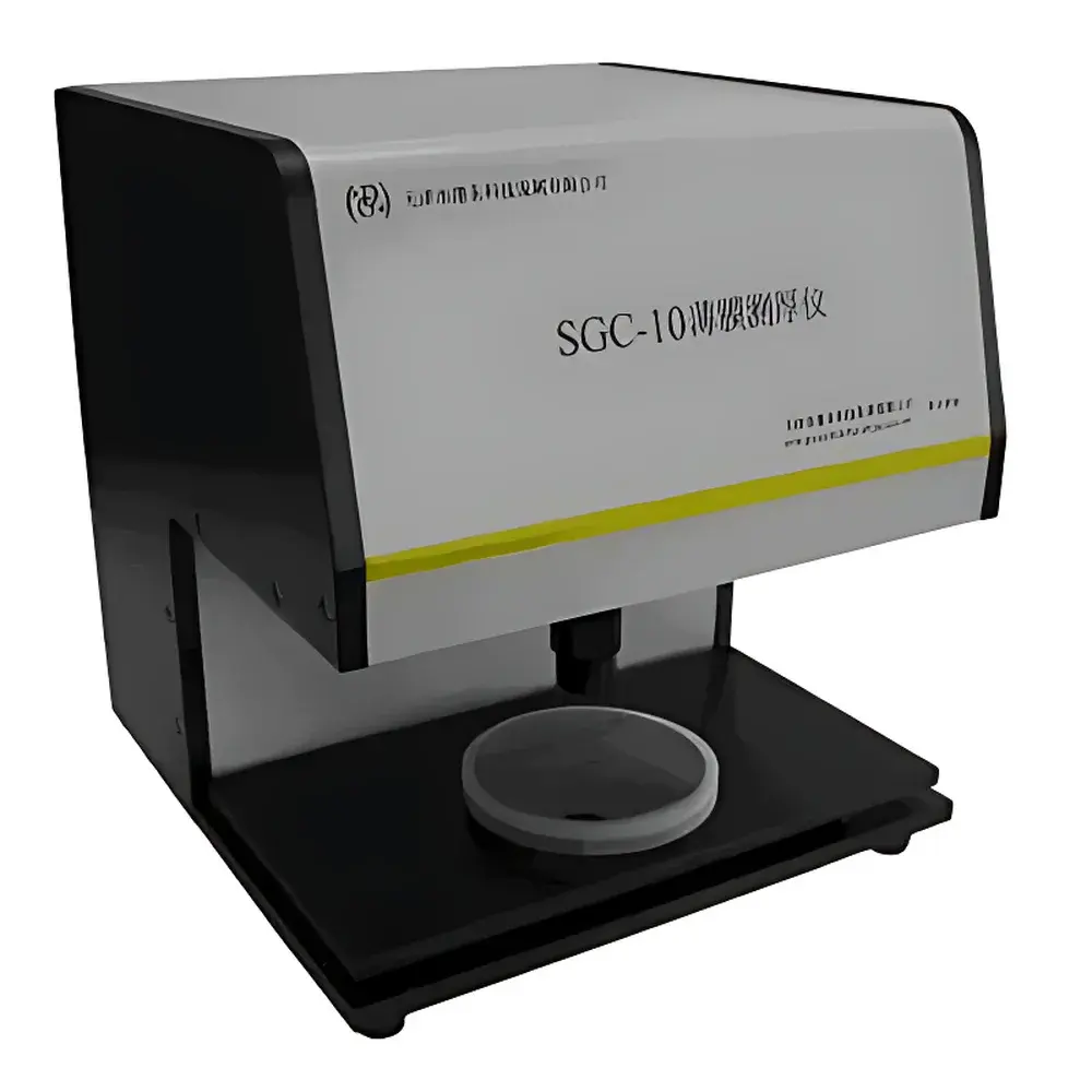
Gangdong SGC-10 White Light Interferometric Thickness Measurement Instrument
| Brand | Gangdong |
|---|---|
| Origin | Tianjin, China |
| Manufacturer Type | Direct Manufacturer |
| Country of Origin | China |
| Model | SGC-10 |
| Price | USD 14,000 (FOB Tianjin) |
| Thickness Range | 20 nm – 50 µm (thickness only) |
| Accuracy | <1 nm or <0.5% |
| Repeatability | 0.1 nm |
| Wavelength Range | 380–1000 nm |
| Max. Layers | 4 |
| Minimum Spot Diameter | 1.2 mm |
| Adjustable Spot Size | 1.2–10 mm |
| Sample Stage | 290 × 160 mm |
| Light Source | Long-life tungsten-halogen lamp (2000 h lifetime) |
| Optical Fiber | Fused silica broadband fiber |
| Detector | Imported fiber-coupled spectrometer |
| Power Supply | AC 100–240 V, 50–60 Hz |
| Dimensions | 300 × 300 × 350 mm |
| Weight | 18 kg |
Overview
The Gangdong SGC-10 White Light Interferometric Thickness Measurement Instrument is a non-contact, high-resolution optical metrology system engineered for precise determination of thin-film thickness and optical constants (refractive index n and extinction coefficient k) in single- and multi-layer film structures. Based on the principle of white light interferometry (WLI), the instrument analyzes spectral interference patterns generated by coherent superposition of light reflected from the film surface and the film–substrate interface. By fitting measured reflectance spectra against theoretical models using rigorous thin-film optics (e.g., transfer matrix method), the SGC-10 delivers quantitative layer-by-layer structural parameters without physical contact or sample destruction. Developed in collaboration with New-Span Inc. (USA), the system integrates core optical components sourced from international suppliers—including a fused silica broadband fiber delivery system, a high-stability tungsten-halogen source (2000 h rated lifetime), and a calibrated fiber-coupled spectrometer—to ensure long-term measurement stability and traceable performance.
Key Features
- Non-destructive, non-contact measurement suitable for delicate, patterned, or temperature-sensitive films
- Simultaneous extraction of thickness (d), refractive index (n), and extinction coefficient (k) for up to four layers per acquisition
- Adjustable spot size (1.2–10 mm diameter) enabling flexibility across macro- and micro-scale regions of interest
- Optimized spectral response across 380–1000 nm, supporting characterization of transparent dielectrics (e.g., SiO2, MgF2), semiconductors (a-Si, poly-Si), and absorbing organics (photoresists, polyimides)
- High repeatability (±0.1 nm) and accuracy (<1 nm or <0.5%, whichever is greater), validated against NIST-traceable reference standards
- Open architecture design: detachable fiber probe compatible with C-mount adapters for integration into upright or inverted microscopes (microscope not included), extending capability to micro-regions (>10 µm resolution dependent on objective magnification)
- Robust mechanical platform with 290 × 160 mm motorized or manual sample stage accommodating wafers, substrates, and coated optical components
Sample Compatibility & Compliance
The SGC-10 supports a broad range of substrate materials including silicon, SiGe, GaAs, sapphire, fused quartz, BK7 glass, ZnS, ZnSe, aluminum-coated acrylic, polycarbonate, and flexible polymer films. It is routinely applied to functional thin films such as antireflection coatings (MgF2, CaF2), passivation layers (SiNx, SiO2), transparent conductive oxides (ITO), dielectric stacks in interference filters, liquid crystal alignment layers, and photoresist profiles in semiconductor process control. The system’s optical model library includes >120 pre-loaded material dispersion datasets (Sellmeier, Cauchy, or Tauc-Lorentz parameterizations), fully editable to accommodate proprietary or novel materials. While not certified to ISO/IEC 17025, the instrument supports GLP-compliant operation through audit-trail-enabled software logging, user-access controls, and exportable raw spectral data compliant with ASTM E2750 and ISO 15630-3 standards for optical thin-film characterization.
Software & Data Management
The embedded Windows-based application provides intuitive workflow navigation—measurement initiation, spectral acquisition, model selection, parameter fitting, and report generation require fewer than five mouse clicks. All raw reflectance spectra are saved in vendor-neutral CSV format; processed results (layer thicknesses, n/k values, confidence intervals, residual error maps) are exportable to Excel, PDF, or XML. The software implements Levenberg–Marquardt nonlinear least-squares fitting with automatic initial parameter estimation and convergence diagnostics. Users may define custom multilayer stack architectures, constrain physical parameters (e.g., fix n for known materials), or perform batch analysis across multiple sites on a single sample. Data integrity is reinforced via timestamped operator logs, version-controlled calibration files, and optional 21 CFR Part 11–compliant electronic signature modules (available as add-on).
Applications
- Process development and endpoint monitoring in PVD, CVD, ALD, spin-coating, and dip-coating lines
- Quality assurance of optical filters, beam splitters, and laser cavity coatings
- R&D of photovoltaic absorber layers (CIGS, perovskites), OLED charge transport layers, and flexible display barriers
- Failure analysis of delamination, interdiffusion, or oxidation-induced thickness drift in packaged MEMS and IC devices
- Academic research in plasmonics, metamaterials, and 2D material heterostructures requiring sub-nanometer thickness resolution
- Calibration and validation of ellipsometers, profilometers, and XRR systems
FAQ
What is the minimum measurable film thickness, and how does material absorption affect sensitivity?
The lower detection limit is 20 nm for highly reflective, low-absorption films (e.g., SiO2/Si). For strongly absorbing films (e.g., metals, amorphous carbon), reliable quantification begins at ~100 nm due to reduced interference contrast.
Can the SGC-10 measure rough or patterned surfaces?
Yes—provided surface roughness RMS < 5% of film thickness and lateral feature pitch exceeds the optical spot size. For structured surfaces, spatial averaging over the illuminated area yields effective optical thickness.
Is vacuum or inert atmosphere operation supported?
No—the standard configuration operates in ambient air. Optional nitrogen purge housing is available for moisture-sensitive hygroscopic films (e.g., certain polymers, perovskites).
How often must the system be recalibrated?
Factory calibration remains stable for ≥12 months under normal lab conditions. Annual verification using certified reference wafers (e.g., Si/SiO2 step standards) is recommended for GMP environments.
Does the system support automated stage mapping or wafer-level scanning?
Manual XY positioning is standard. Motorized stage with programmable grid scan (up to 100 × 100 points) and coordinate-linked reporting is available as an OEM-configurable option.


")
