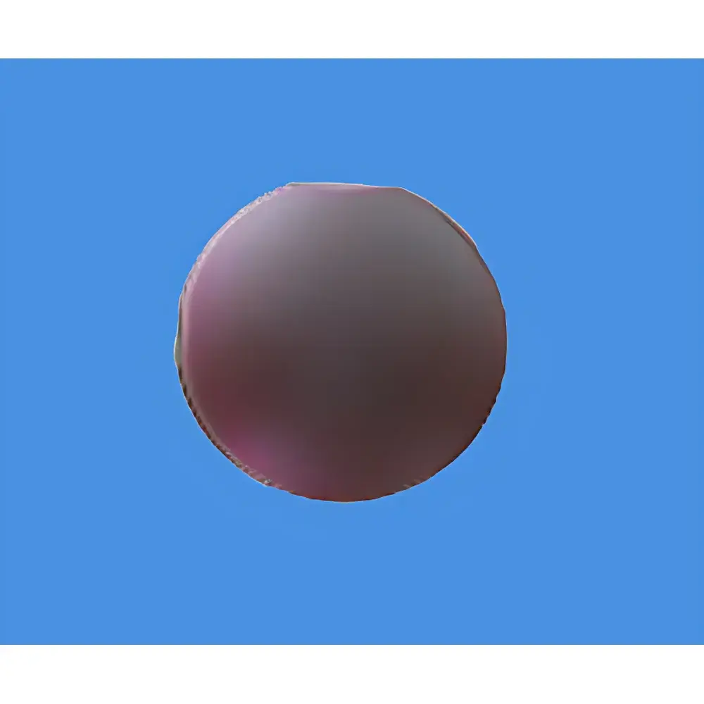
Graphene Film on Ni/SiO₂/Si Substrate
| Brand | 合肥科晶 |
|---|---|
| Origin | USA |
| Manufacturer Type | General Distributor |
| Origin Category | Imported |
| Model | Graphene Film |
| Price | Upon Request |
| Dimensions | Ø100 mm |
| Growth Method | CVD |
| Thickness | 1–10 monolayers |
| Ni Layer Thickness | 300 nm |
| SiO₂ Layer Thickness | 500 nm |
| Si Substrate Thickness | 500 µm |
| Useful Area | ~90% |
| Packaging | Vacuum-sealed in Class 100 cleanroom bag inside Class 1000 cleanroom environment, or individual wafer cassette |
Overview
This graphene film is a high-purity, transfer-free, CVD-grown mono- to few-layer graphene directly synthesized on a structured Ni(300 nm)/SiO₂(500 nm)/Si(500 µm) substrate. Engineered for fundamental research and device prototyping, the film leverages catalytic thermal decomposition of hydrocarbon precursors on nickel under controlled atmospheric conditions—followed by controlled cooling to enable carbon segregation and graphene nucleation at the Ni surface. The underlying SiO₂/Si stack provides mechanical rigidity, optical contrast for microscopy, and compatibility with standard semiconductor metrology tools. Unlike transferred films, this configuration eliminates polymer residue, interfacial contamination, and layer wrinkling commonly introduced during wet-transfer processes—thereby preserving intrinsic electronic, thermal, and optical properties essential for reproducible characterization.
Key Features
- CVD-synthesized graphene with precise control over layer count (1–10 monolayers), verified via Raman spectroscopy and optical contrast analysis
- Integrated Ni(300 nm)/SiO₂(500 nm)/Si(500 µm) heterostructure enabling in situ electrical contact, thermal management, and back-gated transistor configuration
- High uniformity across Ø100 mm wafers with ≥90% usable area—suitable for spatially resolved measurements including micro-Raman mapping and four-point probe resistivity profiling
- Class 100 cleanroom vacuum packaging minimizes adsorbate contamination (H₂O, O₂, hydrocarbons) prior to use, ensuring consistent surface chemistry for UHV-compatible experiments
- Compatible with standard photolithography, electron-beam lithography, and dry etching processes without delamination or interfacial degradation
Sample Compatibility & Compliance
The substrate architecture meets widely adopted dimensional and material specifications for academic and industrial thin-film laboratories. The 500 µm Si thickness conforms to SEM/TEM sample holder standards and enables reliable handling in probe stations and AFM stages. The 500 nm SiO₂ layer provides optimal interference contrast for optical identification of graphene layers under white-light microscopy (per ASTM E2821-22). All substrates are fabricated using trace-metal-controlled sputtering and thermal oxidation processes compliant with ISO 14644-1 Class 5 (ISO Class 5) cleanroom protocols. While not certified for GMP manufacturing, the product is routinely employed in GLP-aligned materials characterization workflows—including carrier mobility extraction per IEEE Std 1620.1™ and sheet resistance measurement per ASTM F390-21.
Software & Data Management
No proprietary software is bundled with this passive material substrate. However, the product is fully interoperable with industry-standard analytical platforms: Raman spectral acquisition systems (e.g., Horiba LabRAM, Renishaw inVia) support automated layer-count mapping using the 2D/G intensity ratio and full-width-at-half-maximum (FWHM) metrics; optical micrographs integrate seamlessly into image analysis suites such as ImageJ/Fiji for area coverage quantification; and electrical transport data acquired via Keithley 4200-SCS or Lake Shore CRX-6.2K cryogenic probe stations can be exported in CSV or HDF5 format for compliance with FAIR data principles. Audit trails for experimental metadata (e.g., ambient humidity, chamber base pressure, laser power) are maintained externally per institutional GLP documentation requirements.
Applications
- Baseline calibration of graphene Raman fingerprinting protocols across instrument platforms
- Development and validation of non-destructive optical and electrical metrology methods for 2D material quality assessment
- Back-gated field-effect transistor (FET) fabrication without transfer-induced defects
- Thermal conductivity modeling using time-domain thermoreflectance (TDTR) on supported graphene
- Surface-enhanced Raman spectroscopy (SERS) substrate development leveraging Ni plasmonic coupling
- Interfacial charge-transfer studies in hybrid perovskite/graphene optoelectronic devices
FAQ
Is this graphene film transferable to other substrates?
No—it is grown directly on the Ni/SiO₂/Si stack and is not designed for wet or dry transfer. Attempting removal will compromise structural integrity and contaminate the graphene lattice.
What is the typical sheet resistance range measured on this film?
Reported values vary with layer count and annealing history; monolayer regions typically yield 300–800 Ω/sq at room temperature under ambient conditions, as confirmed by four-point probe measurements per ASTM F390-21.
Can the Ni layer be etched selectively without damaging the graphene?
Yes—controlled FeCl₃ or ammonium persulfate etching removes Ni while preserving graphene continuity, provided the SiO₂ barrier remains intact. Etch rate must be monitored in real time to avoid undercutting.
Are Raman spectra and optical micrographs included with each shipment?
No—these are reference characterization datasets available upon request for batch verification, not per-unit documentation.
Does the product comply with RoHS or REACH regulations?
The Si and SiO₂ components are inherently compliant; Ni content falls below RoHS threshold limits (≤0.1 wt%). Full REACH SVHC screening documentation is available under NDA upon request.