HalfMoon Model 1 Manual Ellipsometer for Thin-Film Thickness and Optical Constants Measurement
| Brand | HalfMoon |
|---|---|
| Origin | Japan |
| Model | 1 |
| Wavelength Range | 300–800 nm |
| Incident/Reflectance Angle Range | 45°–90° |
| Measurement Method | Rotating Polarizer Element Configuration |
| Sample Stage | Manual Positioning (100 × 100 mm Max) |
| Spectral Detection | Polychromator-Based Multi-Channel Detection (≥400 Wavelength Channels) |
| Angle Drive Mechanism | Sine-Bar Actuated Reflectance Angle Adjustment |
| Optical Constants Output | Refractive Index (n) and Extinction Coefficient (k) |
| Dimensions | 650 H × 400 D × 560 W mm |
| Weight | ~50 kg |
Overview
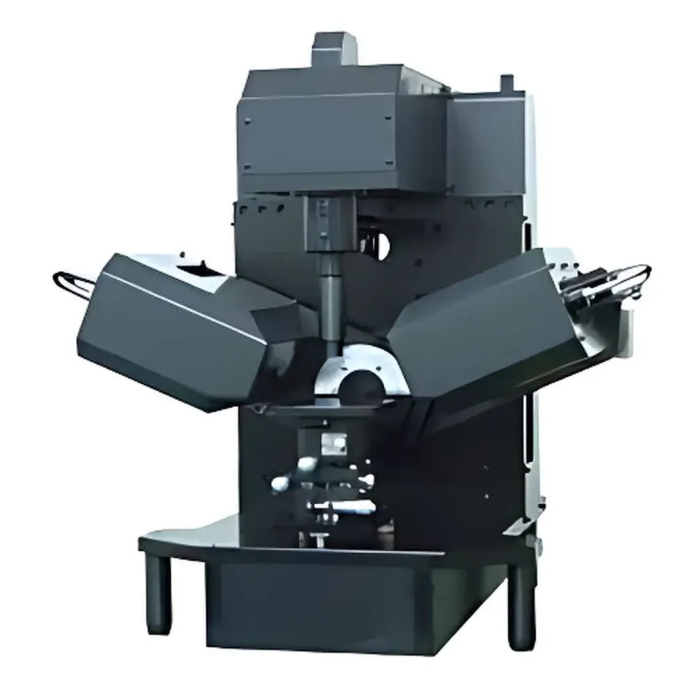
The HalfMoon Model 1 Manual Ellipsometer is a precision optical metrology instrument engineered for non-destructive, contactless characterization of thin films on semiconductor wafers and metallic substrates. It operates on the fundamental principles of spectroscopic ellipsometry—measuring the change in polarization state (amplitude ratio Ψ and phase difference Δ) of light reflected from a sample surface across a broad spectral range (300–800 nm). Unlike single-wavelength or scanning monochromator-based systems, this ellipsometer employs a polychromator architecture enabling simultaneous acquisition of ≥400 wavelength channels, significantly reducing measurement time while preserving spectral fidelity. Designed for laboratory-scale R&D and process validation—not high-throughput production—the system delivers high reproducibility in determining film thickness (sub-nanometer resolution), refractive index (n), and extinction coefficient (k) for single-layer and multi-layer dielectric, semiconductor, and metallic films. Its manual sample handling and fixed-stage configuration prioritize optical stability and alignment integrity over automation, making it especially suitable for controlled environment labs where operator intervention supports rigorous calibration traceability and experimental flexibility.
Key Features
- Spectroscopic detection via high-throughput polychromator, delivering full-spectrum ellipsometric data (Ψ, Δ) in a single acquisition cycle
- Sine-bar actuated reflectance angle drive mechanism ensuring sub-arcminute repeatability during angular sweeps from 45° to 90°
- Rotating polarizer element configuration—robust, low-drift optical design minimizing polarization artifacts from compensator degradation
- Simultaneous multi-angle measurement capability: enables rapid acquisition of angular dispersion datasets critical for anisotropic film modeling
- Optimized optical path for both wafer-level (up to 100 × 100 mm) and small-area metallic substrate analysis without beam reconfiguration
- Thermally stabilized optical bench and rigid aluminum frame minimizing mechanical drift during extended acquisitions
Sample Compatibility & Compliance
The HalfMoon Model 1 accommodates flat, optically reflective samples up to 100 × 100 mm in dimension—including silicon wafers (bare or oxide-coated), sapphire substrates, patterned metal films (Al, Cu, TiN), and transparent conductive oxides (ITO, AZO). Surface roughness should remain below 1 nm RMS for reliable n/k extraction; thicker or highly absorbing films (>500 nm) require multi-layer optical modeling using Cauchy or Tauc-Lorentz dispersion relations. The instrument complies with ISO 15504-3 (optical thin-film measurement standards) and supports traceable calibration protocols aligned with NIST-traceable reference standards (e.g., Si/SiO₂ certified thickness wafers). While not FDA 21 CFR Part 11–validated out-of-the-box, its raw data export format (ASCII .csv and binary .el3) permits integration into GLP/GMP-compliant LIMS environments when paired with validated third-party analysis software.
Software & Data Management
The system ships with HalfMoon Ellipsometry Suite v4.x—a Windows-based application supporting real-time spectrum visualization, interactive Ψ/Δ fitting, and library-driven optical model construction (e.g., bulk substrate + Cauchy layer + roughness layer). All raw detector intensities, motor position logs, and environmental metadata (ambient temperature, humidity timestamp) are stored in hierarchical HDF5 containers, ensuring audit-ready data provenance. Export options include ASTM E2927-compliant reports, CSV tables for external regression (e.g., MATLAB, Python SciPy), and image-mapped thickness maps when used with optional XY translation stages (not included). Software updates are distributed via secure HTTPS portal; no cloud synchronization or telemetry is enabled by default.
Applications
- Process development of ALD and PECVD dielectric stacks (SiO₂, SiNₓ, HfO₂) on 200 mm wafers
- Quantification of native oxide growth kinetics on polished Al and Cu interconnects
- Characterization of optical constants for emerging 2D materials (MoS₂, WS₂) exfoliated onto SiO₂/Si
- Thickness uniformity mapping of spin-coated photoresists pre- and post-bake
- Validation of optical models used in TCAD simulation input parameterization
- Failure analysis of delamination interfaces via complex refractive index contrast profiling
FAQ
Is automated stage positioning available?
No—the Model 1 is manually operated for sample loading and coarse alignment. Precision angular control is automated, but lateral/vertical positioning requires manual adjustment using calibrated micrometer stages.
Can it measure transparent conductive oxides on glass?
Yes, provided the glass substrate has known optical constants and surface flatness meets λ/10 specification at 633 nm.
What calibration standards are recommended?
NIST-traceable Si/SiO₂ step-height standards (e.g., VLSI Standards SRM 2001) and certified quartz reference plates for wavelength accuracy verification.
Does the system support Mueller matrix measurements?
No—it implements a two-zone rotating polarizer configuration optimized for Ψ/Δ retrieval, not full Mueller matrix acquisition.
Is vacuum or inert atmosphere operation possible?
The base configuration is ambient-air only; optional purge ports and O-ring sealed chamber adaptation kits are available upon request for nitrogen-purged environments.


