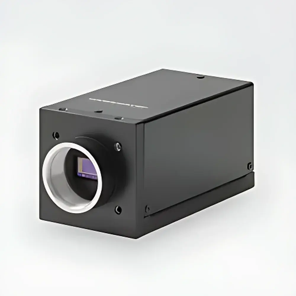
Hamamatsu C15333-10E04-02 InGaAs Linear SWIR Camera
| Brand | Hamamatsu |
|---|---|
| Origin | Japan |
| Manufacturer Type | Original Equipment Manufacturer (OEM) |
| Product Category | Imported |
| Model | C15333-10E04-02 |
| Effective Pixels | 1024 (H) × 1 (V) |
| Pixel Size | 12.5 µm (H) × 12.5 µm (V) |
| Spectral Range | 950–1700 nm |
| Max Line Rate | 40 kHz (internal trigger), 20 kHz (edge trigger) |
| Output Bit Depth | 14-bit |
| Interface | Gigabit Ethernet |
| Exposure Time | 21 µs to 1 s |
| Power Supply | DC 12 V |
| Max Power Consumption | 6 W |
| Operating Temperature | 0–40 °C |
| Humidity Range (Operating) | 30–80% RH (non-condensing) |
| Lens Mount | C-mount |
| Trigger Inputs | SMA or 12-pin Hirose connector |
| Onboard Image Processing | Background subtraction, real-time shading correction, pixel inversion |
Overview
The Hamamatsu C15333-10E04-02 is a high-performance InGaAs linear array short-wave infrared (SWIR) scanning camera engineered for precision industrial inspection and scientific imaging applications. Operating across the 950–1700 nm spectral band, it leverages the intrinsic optical transparency of silicon, plastics, and organic materials in the SWIR region—enabling non-destructive, subsurface visualization that is inaccessible to visible-light or near-infrared (NIR) sensors. Unlike area-scan CCD or CMOS imagers, this line-scan architecture delivers high-speed, continuous-motion imaging ideal for inline manufacturing environments. Its 1024-pixel linear sensor—with uniform 12.5 µm pitch and optimized quantum efficiency—ensures high spatial resolution and radiometric consistency across the full field. The camera implements a true analog-to-digital signal chain with 14-bit digitization, preserving dynamic range for quantitative reflectance and transmission analysis. Designed for integration into automated optical inspection (AOI) systems, it supports deterministic timing via hardware-triggered acquisition, making it suitable for use with variable-speed conveyors, rotating stages, or synchronized laser illumination sources.
Key Features
- InGaAs linear sensor with 1024 × 1 active pixels and 12.5 µm × 12.5 µm pixel pitch, delivering 12.8 mm effective scan width
- Extended SWIR spectral response from 950 nm to 1700 nm—optimized for silicon wafer inspection, moisture detection, and polymer identification
- Maximum line rate of 40 kHz in internal trigger mode (21 µs exposure), and 20 kHz under edge-triggered operation for robust synchronization with motion profiles
- Dual trigger capability: edge-trigger input for adaptive frame capture upon object arrival, and synchronous readout trigger for precise multi-camera or multi-sensor coordination
- Onboard real-time image processing including background subtraction and shading correction—reducing post-acquisition computational load and improving measurement repeatability
- Gigabit Ethernet interface compliant with IEEE 802.3, enabling deterministic data streaming up to 120 MB/s with low-latency packet delivery and integrated TCP/IP stack
- C-mount lens interface for compatibility with standard SWIR-optimized optics; optional lens adapters available for telecentric or macro configurations
- Compact, fanless mechanical design rated for continuous operation at ambient temperatures from 0 °C to +40 °C and relative humidity up to 80% non-condensing
Sample Compatibility & Compliance
The C15333-10E04-02 is validated for use in regulated industrial and research environments requiring traceable, repeatable imaging performance. Its spectral sensitivity enables direct inspection of silicon-based substrates without sample preparation—supporting ISO 10110-7 (optical component surface quality) and SEMI F20 (silicon wafer metrology) workflows. In food and pharmaceutical packaging inspection, the camera complies with requirements for non-contact, non-ionizing evaluation per FDA Guidance for Industry on Process Validation (2011) and supports GLP-compliant documentation when integrated with audit-trail-enabled host software. All electrical interfaces meet IEC 61000-6-2 (immunity) and IEC 61000-6-4 (emissions) standards. No laser safety classification applies, as the device is purely passive; however, system-level integration must adhere to IEC 60825-1 if used with auxiliary illumination sources.
Software & Data Management
Hamamatsu provides the official C15333 Series SDK for Windows and Linux platforms, supporting C/C++, Python (via ctypes bindings), and MATLAB interfaces. The SDK includes low-level register access, asynchronous acquisition control, and configurable trigger routing—enabling custom synchronization logic for multi-axis motion systems. Image data streams are delivered in raw 14-bit format over GigE Vision-compliant protocols, ensuring interoperability with third-party machine vision frameworks such as HALCON, OpenCV, and Common Vision Blox. Built-in metadata tagging includes timestamp (µs resolution), exposure duration, gain setting, and sensor temperature—facilitating time-series correlation and statistical process control (SPC) analysis. For compliance-critical deployments, the SDK supports optional integration with FDA 21 CFR Part 11–compliant electronic signature modules through certified middleware partners.
Applications
- Food & Agriculture: Detection of foreign bodies (e.g., plastic fragments in dried fruit), bruise mapping in apples and potatoes, moisture content quantification in grains, and fill-level verification in opaque beverage containers
- Semiconductor Manufacturing: High-throughput inspection of photolithographic patterns on silicon wafers, electroluminescence (EL) and photoluminescence (PL) imaging of solar cells, and defect localization in bonded SOI substrates
- Industrial Quality Control: Seal integrity verification in blister packs, coating thickness estimation on polymer films, leak detection in sealed metal cans via thermal transmittance anomalies, and fiber orientation analysis in composite laminates
- Research & Development: Spectral reflectometry of novel 2D materials, hyperspectral line-scan calibration reference, and time-resolved pump-probe imaging in ultrafast optics laboratories
FAQ
What is the maximum usable line rate when using external edge triggering?
The maximum sustained line rate under edge-triggered acquisition is 20 kHz, corresponding to a minimum inter-line interval of 50 µs—including exposure (21 µs), readout, and reset phases.
Does the camera support pixel binning or region-of-interest (ROI) readout?
No—this is a fixed 1024-pixel linear sensor with full-frame readout only; ROI or binning is not implemented in hardware or firmware.
Can the background subtraction be applied in real time during acquisition?
Yes—background reference frames are captured and stored onboard, and subtraction is performed in FPGA prior to digitization and GigE transmission.
Is lens calibration data provided by Hamamatsu?
Hamamatsu supplies MTF curves and spectral responsivity data for its recommended SWIR lenses (e.g., Saini Optics SWIR-C series); geometric distortion maps require user-side characterization using standard checkerboard targets.
What power supply ripple tolerance does the camera specify?
The unit requires a stable DC 12 V ±5% supply with peak-to-peak ripple ≤50 mV; excessive noise may induce fixed-pattern noise or timing jitter in triggered modes.


