Hamamatsu Dual PHEMOS®-X Ultra-Low-Light Microscope C16506-01
| Brand | Hamamatsu |
|---|---|
| Origin | Japan |
| Manufacturer | Hamamatsu Photonics K.K. |
| Type | Imported Instrument |
| Model | C16506-01 |
| Pricing | Upon Request |
Overview
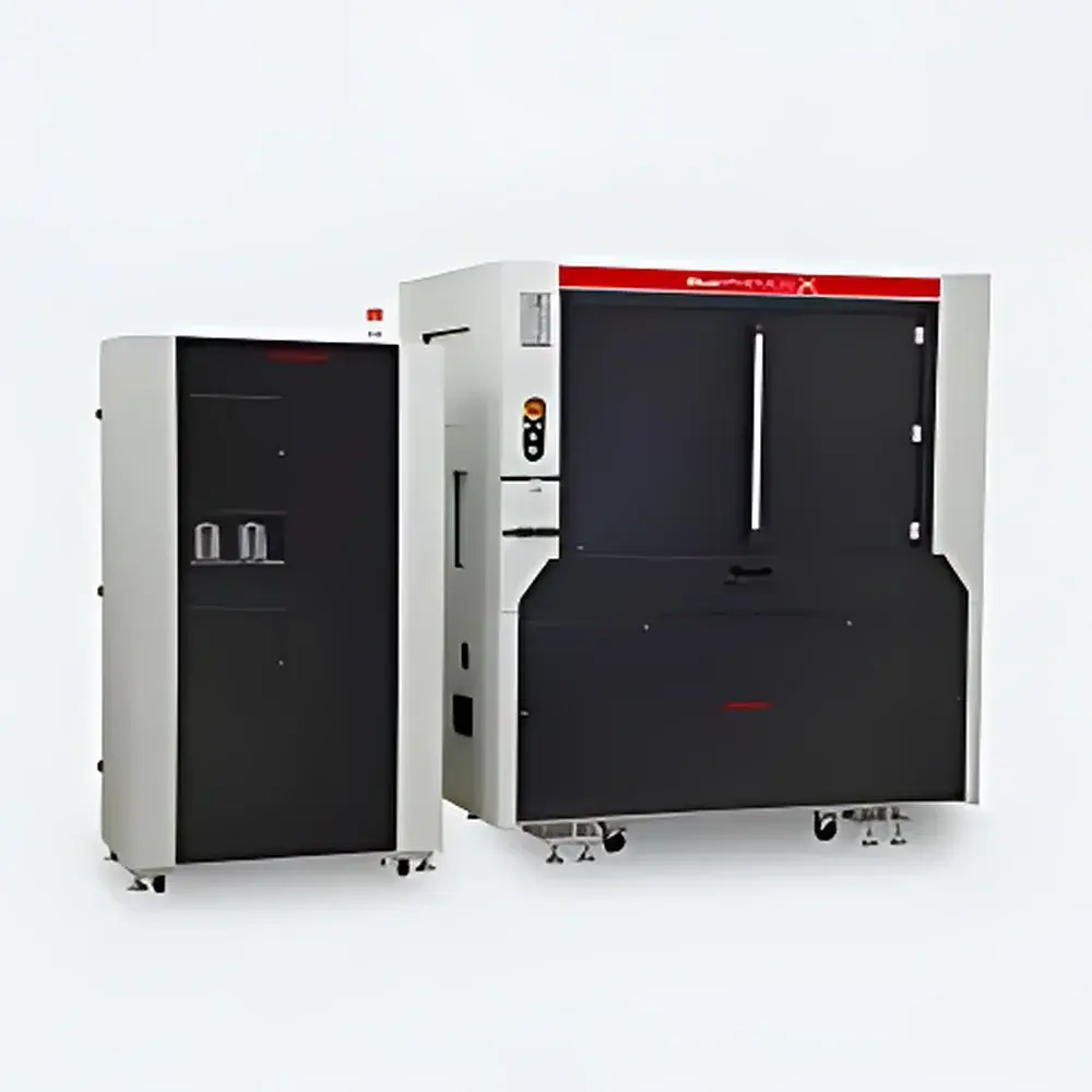
The Hamamatsu Dual PHEMOS®-X Ultra-Low-Light Microscope (Model C16506-01) is a purpose-built optical failure analysis platform engineered for advanced 3D non-transparent semiconductor devices—particularly stacked-die packages, through-silicon via (TSV) interposers, and heterogeneous integration structures where electrical faults may originate from either the frontside (top) or backside (bottom) of the die. Unlike conventional photon emission microscopes (PEMs), the Dual PHEMOS-X integrates dual-sided optical access within a single, co-registered mechanical architecture, enabling simultaneous or rapid sequential top/bottom photon detection without sample relocation or system reconfiguration. Its core measurement principle relies on high-sensitivity, time-gated intensified CCD (ICCD) imaging optimized for sub-picoamp leakage currents and localized hot-carrier-induced photon emission (e.g., near-infrared to visible wavelengths, ~400–1100 nm). This enables precise spatial correlation of electroluminescence (EL) and thermally activated photon emission (TIA/TAPE) signals with device layout data—critical for root-cause identification in FinFET, GAA, and advanced packaging nodes.
Key Features
- Dual-sided optical access: Integrated top and bottom objective paths with independent focus, alignment, and illumination control—eliminating cross-system transfer and preserving positional fidelity between frontside and backside FA sessions.
- High-precision XYZθ motorized stage: Top-side stage travel (40 × 40 × 80 mm) and bottom-side stage travel (60 × 60 × 20 mm) support full-wafer (up to 300 mm) and diced-die inspection; compatible with semi-automated probe station MPd-1000X (C16688-01) for electrical stimulation during photon capture.
- Multi-modal image fusion: Real-time overlay of ultra-low-light emission images onto high-resolution optical or SEM reference patterns—enabling sub-micron defect localization with contextual layout registration.
- Advanced visualization suite: Includes split-screen display (up to six synchronized windows), scalable grid/coordinate overlays, user-annotatable markers (arrows, text, regions of interest), segmented scale bars, thumbnail-based image library management, and dynamic contrast enhancement algorithms optimized for low-SNR photon maps.
- Robust environmental integration: Designed for cleanroom-compatible operation with vacuum-assisted sample stabilization (−40 to −80 kPa), regulated compressed air interface (0.5–0.7 MPa), and dual-rack power architecture supporting stable ICCD gating under variable load conditions (system rack: ~3300 VA; probe station rack: ~4400 VA).
Sample Compatibility & Compliance
The Dual PHEMOS-X accommodates bare dies, packaged ICs (QFN, BGA, WLCSP), and full 200 mm / 300 mm wafers mounted on standard probe station chucks or custom backgrinding carriers. Its mechanical design complies with SEMI S2/S8 safety standards for semiconductor manufacturing equipment. Image acquisition workflows support audit-ready documentation per ISO/IEC 17025 requirements, and metadata logging—including stage coordinates, exposure parameters, gate timing, and stimulus conditions—is fully traceable for GLP/GMP-aligned failure analysis reporting. While not FDA-certified (as it is not a medical device), its data integrity framework aligns with principles outlined in FDA 21 CFR Part 11 for electronic records and signatures when integrated with validated laboratory information management systems (LIMS).
Software & Data Management
Control and analysis are executed via Hamamatsu’s proprietary PHEMOS-X software suite (v5.x or later), which provides scriptable automation for wafer mapping, auto-focus sequences, multi-point photon counting, and time-resolved emission profiling. All acquired images retain embedded EXIF-style metadata: timestamp, stage position (X/Y/Z/θ), objective magnification, ICCD gain/integration time, and electrical stimulus profile (voltage/current waveform ID). Export formats include TIFF (16-bit linear), PNG (lossless), and HDF5 for quantitative pixel-intensity analysis. The software supports DICOM-like structured annotation export and integrates with industry-standard FA databases via CSV/XML APIs—facilitating traceability across yield analysis, reliability testing, and cross-functional debug workflows.
Applications
- Root-cause analysis of gate oxide breakdown (GOX), junction leakage, and latch-up events in logic and memory devices.
- Backside fault isolation in thinned silicon or silicon-on-insulator (SOI) substrates using laser-assisted photon emission (LAPE) or thermal laser stimulation (TLS).
- Electrical validation of TSV interconnect integrity and microbump reliability in 2.5D/3D IC stacks.
- Correlation of photon emission hotspots with layout-aware physical verification (e.g., DRC/LVS mismatches, metal density violations).
- Qualification of low-power IoT and automotive-grade SoCs under dynamic voltage/frequency scaling (DVFS) stress conditions.
FAQ
Is the Dual PHEMOS-X compatible with third-party probe stations?
Yes—mechanical and electrical interfaces comply with standard SEMI E10/E120 mounting specifications; however, full synchronization of stimulus triggering and image gating requires Hamamatsu’s MPd-1000X (C16688-01) or certified OEM integrations.
What is the minimum detectable photon flux under typical operating conditions?
Detection sensitivity is instrument-configuration-dependent; with standard 50× objective and 1 s gated integration, the system achieves <100 photons/pixel/s at SNR ≥ 3 for 850 nm emission—validated per Hamamatsu internal test protocol H-PHEMOS-TS-004.
Does the system support automated wafer-level photon mapping?
Yes—integrated wafer mapping functionality includes die-level coordinate referencing, pattern recognition-assisted alignment, and batch export of emission intensity heatmaps aligned to GDSII layer data.
Can emission images be correlated with CAD layout files?
Yes—the software imports GDSII/OASIS files and performs real-time geometric transformation (rotation, scaling, offset compensation) to overlay photon data onto design layers with sub-µm registration accuracy.
What maintenance intervals are recommended for the ICCD detector?
Hamamatsu recommends annual calibration and vacuum integrity verification; the ICCD tube lifetime exceeds 10,000 hours under nominal gating duty cycles (<10% duty factor).


