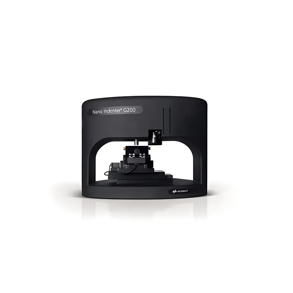
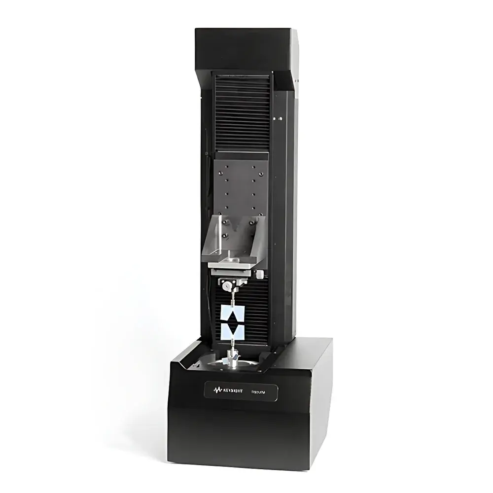
Keysight G200 / iMicro / iNano / InSEM Micro- and Nanoindentation Testing Systems
| Brand | Keysight Technologies |
|---|---|
| Origin | USA |
| Model Series | G200, iMicro, iNano, InSEM |
| Application Domain | In-situ Mechanical Characterization, Dynamic & Static Nanoindentation, Multi-modal Correlative Analysis |
Overview
The Keysight G200, iMicro, iNano, and InSEM micro- and nanoindentation systems represent the industry benchmark for quantitative mechanical property characterization at sub-micron to nanoscale length scales. Engineered on the foundational principles of depth-sensing indentation (DSI), these instruments employ high-resolution capacitive displacement transducers and low-noise electrostatic force actuation to measure load–displacement curves with sub-nanometer depth resolution and sub-micronewton force sensitivity. The core measurement methodology adheres to ISO 14577 (Metallic materials — Instrumented indentation test) and ASTM E2546 (Standard Test Method for Instrumented Indentation Testing), enabling traceable determination of hardness (H), reduced modulus (Er), creep compliance, and strain-rate sensitivity. Critically, Keysight’s proprietary Continuous Stiffness Measurement (CSM) technology—now codified in GB/T 22458 (Chinese National Standard for Instrumented Indentation Testing)—enables real-time, cycle-by-cycle stiffness evaluation during oscillatory loading, facilitating accurate modulus mapping even on compositionally graded or heterogeneous surfaces.
Key Features
- CSM Technology Integration: Real-time stiffness acquisition via superimposed small-amplitude harmonic oscillation (typically 45–100 Hz) on quasi-static loading ramps; supports modulus mapping with spatial resolution down to 100 nm.
- Multi-platform Architecture: G200 (benchtop, high-force range up to 500 mN), iMicro (compact, optimized for thin films and coatings), iNano (ultra-high resolution, <1 nN force noise floor), and InSEM (fully integrated into scanning electron microscopes for correlative nano-mechanical + structural + compositional analysis).
- In-situ Multimodal Capability: Synchronized operation with optical microscopy, SEM/EDS, Raman spectroscopy, and electrical probing stages—enabling concurrent mechanical response, topographic evolution, phase identification, and local conductivity assessment.
- Dynamic Testing Modes: Includes creep, stress relaxation, cyclic indentation, and rate-jump experiments compliant with ISO 14577-3 for time-dependent mechanical behavior quantification.
- Robust Environmental Control: Optional vacuum, temperature-controlled stages (−120 °C to +300 °C), and humidity chambers for testing under non-ambient conditions relevant to semiconductor packaging, battery electrode mechanics, and biomaterial stability studies.
Sample Compatibility & Compliance
These systems accommodate a broad spectrum of solid-state specimens—including single crystals, polycrystalline metals, ceramics, polymers, thin-film stacks, MEMS devices, and biological tissues—without requiring conductive coating (unlike many SEM-integrated alternatives). Sample height tolerance spans 0–100 mm; maximum sample weight is 5 kg. All models comply with CE marking requirements and meet electromagnetic compatibility (EMC) standards per IEC 61326-1. Data integrity protocols align with FDA 21 CFR Part 11 for audit trails, electronic signatures, and secure user access control—supporting GLP/GMP-regulated environments in pharmaceutical excipient development and medical device validation.
Software & Data Management
TriboScan™ software provides unified control across all platform variants, featuring scriptable test sequences, automated grid mapping, and batch processing for high-throughput screening. Raw load–displacement data are stored in HDF5 format with embedded metadata (timestamp, operator ID, calibration history, environmental logs). Built-in analysis modules implement Oliver–Pharr methodology, Sneddon solutions for conical indenters, and custom fitting routines for viscoelastic and plastic constitutive modeling. Export options include CSV, MATLAB .mat, and MTEX-compatible formats for crystallographic orientation–mechanical property correlation. Audit logs record all parameter modifications and data exports, satisfying ISO/IEC 17025 documentation requirements for accredited testing laboratories.
Applications
- Mechanical property gradients in thermal barrier coatings and weld heat-affected zones
- Hardness and modulus mapping of semiconductor interconnects and 3D NAND stack layers
- Creep behavior of polymer electrolytes in solid-state batteries under thermal bias
- Nano-scale fracture toughness estimation via indentation-induced cracking in brittle oxides
- In-situ mechanical degradation monitoring of hydrogels during swelling or enzymatic digestion
- Correlative nano-mechanics and phase imaging in multiphase alloys using InSEM + EBSD synchronization
FAQ
What distinguishes CSM from conventional static nanoindentation?
CSM enables continuous, high-frequency stiffness sampling during loading, eliminating reliance on unloading curve fitting alone—critical for materials exhibiting significant pile-up, sink-in, or time-dependent deformation.
Can the InSEM system operate inside high-vacuum SEM chambers?
Yes—the InSEM is engineered for ultra-high vacuum compatibility (≤1×10⁻⁶ Pa) and includes differential pumping interfaces to maintain chamber integrity while enabling nanomechanical actuation.
Is tribochemical wear simulation supported?
While not a dedicated tribometer, the iNano and G200 support scratch testing with lateral force measurement and in-situ acoustic emission detection—enabling qualitative wear onset analysis and coefficient-of-friction estimation.
How is instrument calibration verified?
Keysight-certified calibration uses NIST-traceable reference materials (e.g., fused silica, sapphire, and certified hardness standards) with annual recalibration recommended per ISO/IEC 17025 Clause 6.5.
Does the software support custom indenter geometry modeling?
Yes—TriboScan allows user-defined tip shape functions (e.g., Berkovich, cube-corner, spherical, or custom polynomial profiles) for accurate contact area function derivation and modulus correction.
")


