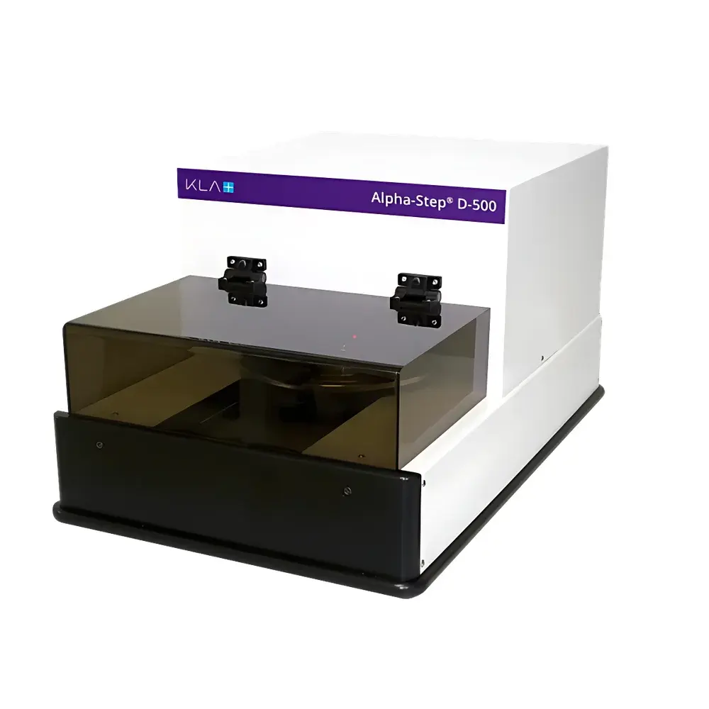
KLA Alpha-Step D500 Profilometer
| Brand | KLA |
|---|---|
| Origin | Guangdong, China |
| Manufacturer Type | Authorized Distributor |
| Product Origin | Domestic (China) |
| Model | D500 |
| Price Range | USD 42,000 – 56,000 (FOB) |
| Measurement Principle | Optical Lever-Based Contact Profilometry |
| Vertical Measurement Range | 10 nm – 1000 µm |
| Vertical Accuracy | ±0.01% of full-scale range |
| Probe Tip Radius | 2 µm |
| Adjustable Normal Force | 0.03–15 mg |
| Maximum Single-Scan Length | 30 mm |
| Step Height Repeatability | 0.5 nm (RMS, measured on 1 µm SiO₂ step standard over 15 repeated scans) |
| Vertical Resolution | 0.038 nm |
| Maximum Sample Size | 140 mm diameter circular stage |
Overview
The KLA Alpha-Step D500 is a high-precision, optical lever-based contact profilometer engineered for quantitative 2D surface topography characterization in semiconductor process development, MEMS fabrication, thin-film metrology, and advanced packaging R&D environments. Unlike optical interferometric or confocal methods, the D500 employs a mechanically scanned stylus coupled with a quadrant photodetector and precision optical lever amplification—enabling direct, traceable displacement measurement independent of sample optical properties (e.g., reflectivity, transparency, or absorption). This principle ensures consistent performance across diverse materials including silicon, SiO₂, SiNₓ, photoresists, metals, polymers, and low-k dielectrics. The instrument delivers sub-angstrom vertical resolution and nanometer-level repeatability while maintaining a wide dynamic range—critical for characterizing both atomic-scale roughness and micron-scale wafer bow or film stress-induced curvature.
Key Features
- Optical lever sensor architecture with 0.038 nm vertical resolution and 0.5 nm RMS step height repeatability on certified 1 µm reference standards
- Programmable normal force control (0.03–15 mg) to minimize surface deformation on soft films, photoresists, or compliant substrates
- 2 µm radius diamond-tipped probe optimized for high aspect-ratio feature profiling without tip wear-induced artifacts
- 30 mm maximum single-scan length with motorized X-stage and closed-loop position feedback for precise lateral registration
- 140 mm diameter vacuum chuck stage supporting full-wafer and large-area substrate handling with repeatable Z-axis leveling
- Integrated thermal drift compensation and vibration-isolated granite base for long-duration measurements under ambient lab conditions
Sample Compatibility & Compliance
The Alpha-Step D500 accommodates a broad spectrum of sample geometries and material systems—including bare wafers, patterned reticles, glass substrates, flexible OLED panels, and ceramic packages. Its contact-based methodology eliminates ambiguity associated with optical edge detection or coherence envelope interpretation. The system supports ASTM E1399 (Standard Test Method for Measuring Thickness of Thin Films Using a Stylus Profilometer), ISO 25178-2 (Geometrical Product Specifications – Surface Texture), and SEMI MF1530 (Test Method for Measuring Thin Film Thickness by Stylus Profilometry). Data acquisition and reporting comply with GLP/GMP documentation requirements; audit trails, user access logs, and electronic signatures can be enabled per FDA 21 CFR Part 11 configuration guidelines when integrated with validated LIMS or MES platforms.
Software & Data Management
The D500 operates with KLA’s proprietary Alpha-Step Analysis Software (v5.2+), providing calibrated cross-sectional analysis, multi-point roughness calculation (Ra, Rq, Rz, Rsk, Rku), film stress derivation via Stoney’s equation, and automated step height quantification with edge-detection thresholding and baseline fitting algorithms. All raw profile data are stored in vendor-neutral ASCII format with embedded metadata (timestamp, operator ID, calibration status, environmental conditions). Batch processing, report templating (PDF/Excel), and API-driven export enable integration into automated yield analysis workflows. Software validation documentation (IQ/OQ/PQ protocols) is available upon request for regulated manufacturing environments.
Applications
- Quantifying etch depth, deposition thickness, and lithographic CD uniformity in front-end-of-line (FEOL) and back-end-of-line (BEOL) processes
- Measuring post-CMP dishing and erosion on interlayer dielectric stacks
- Characterizing surface roughness evolution during ALD/PECVD film growth and thermal annealing
- Determining residual stress in thin films (e.g., TiN, TaN, SiNₓ) using wafer curvature analysis
- Validating MEMS release etch completeness and sidewall profile fidelity
- Assessing coating uniformity and edge exclusion on display-grade glass and flexible substrates
FAQ
Is the Alpha-Step D500 suitable for measuring soft polymer films without indentation artifacts?
Yes—the ultra-low force range (0.03–15 mg) and programmable approach/retract velocity allow non-destructive profiling of photoresists, PI, BCB, and other organic layers.
Can the system measure steps higher than 1000 µm?
No—the specified vertical range is 10 nm to 1000 µm; for larger topographies, users may employ stitching or multi-range scanning with manual stage repositioning.
Does the D500 support automated wafer mapping?
Not natively—the system is optimized for localized site-specific measurements; full-wafer mapping requires integration with third-party robotic handlers and custom scripting.
What calibration standards are recommended for routine verification?
NIST-traceable step height standards (e.g., NIST SRM 2160, 2161) and roughness standards (e.g., VDI/VDE 2634 Part 2) are supported; KLA provides annual recalibration services with ISO/IEC 17025-accredited certificates.
Is the software compatible with Windows 10/11 64-bit operating systems?
Yes—Alpha-Step Analysis Software v5.2 and later are validated on Windows 10 Pro (22H2) and Windows 11 Enterprise (23H2) with .NET Framework 4.8 and DirectX 12 runtime dependencies.