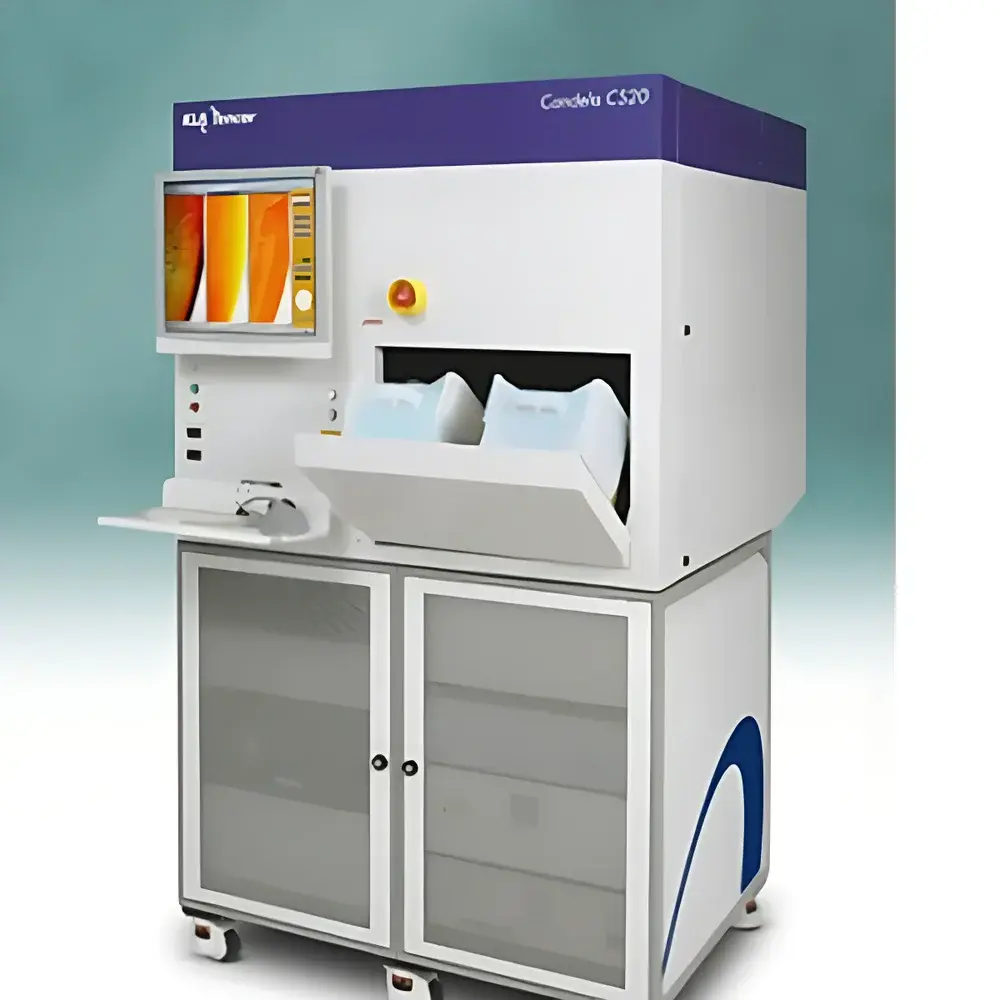
KLA Candela CS20 Wafer Surface Defect Inspection System
| Brand | KLA |
|---|---|
| Origin | Singapore |
| Manufacturer Type | Authorized Distributor |
| Origin Category | Imported |
| Model | CS20 |
| Quotation | Upon Request |
| Instrument Category | Optical Non-Patterned Wafer Defect Inspection System |
| Primary Application | Bare (Non-Patterned) Silicon Wafer Surface Defect Detection |
| Throughput | 30 WPH for 150 mm (6″) wafers, 27 WPH for 200 mm (8″) wafers |
| Resolution | 83 nm |
| Substrate Diameter Range | 50.8 mm – 200 mm (2″ – 8″) |
| Thickness Range | 350 µm – 1,100 µm |
| Minimum Detectable Defect Size | 0.3 µm (PSL sphere equivalent, ≥95% capture rate on bare Si) |
| Defect Types | Particles, scratches (≥100 µm × 0.1 µm × 50 Å), pits (≥20 µm Ø × 50 Å depth), stains (≥20 µm Ø × 10 Å thickness), bumps |
| Detection Threshold | Signal amplitude > 3× peak-to-valley background noise |
Overview
The KLA Candela CS20 Wafer Surface Defect Inspection System is a high-sensitivity, automated optical inspection platform engineered for rapid, non-destructive detection of surface anomalies on bare (non-patterned) semiconductor wafers. Leveraging advanced dark-field laser scattering imaging with optimized illumination geometry and high-dynamic-range CCD detection, the CS20 identifies sub-micron defects—including particles, scratches, pits, stains, and micro-bumps—based on their characteristic light-scattering signatures. Its design adheres to the fundamental principles of elastic light scattering from surface perturbations, where defect contrast arises from localized deviations in surface reflectivity, topography, or material composition. The system is purpose-built for front-end process control in silicon wafer manufacturing, epitaxial layer evaluation, and pre-epi/post-CMP incoming inspection workflows—serving as a critical gatekeeper prior to lithography or thin-film deposition steps.
Key Features
- Sub-100 nm lateral resolution (83 nm specified) enabled by precision optical alignment, high-numerical-aperture collection optics, and stabilized multi-angle laser illumination
- Configurable substrate handling for 2″–8″ (50.8–200 mm) wafers, supporting thicknesses from 350 µm to 1,100 µm without mechanical reconfiguration
- Dual-mode detection architecture: simultaneous bright-field and dark-field imaging for enhanced defect signature discrimination
- Automated defect classification engine trained on physics-based scattering models and empirical defect libraries, delivering ≥95% capture rate for 0.3 µm polystyrene latex (PSL) spheres on bare silicon
- Robust signal-to-noise architecture ensuring detection threshold compliance: all reported defects exhibit signal amplitude exceeding 3× peak-to-valley background variation
- Integrated vacuum chuck with edge exclusion masking and real-time focus tracking for consistent image fidelity across full wafer maps
Sample Compatibility & Compliance
The CS20 accommodates any opaque, polished substrate exhibiting ≥10% diffuse scattering efficiency—including bare silicon, sapphire, SiC, GaN, and SOI wafers—as well as select transparent substrates meeting the same scattering criterion. It supports both front-side and back-side inspection without hardware modification. From a regulatory and quality systems perspective, the platform’s data acquisition and reporting architecture is compatible with GLP/GMP environments: raw image metadata, defect coordinates, intensity histograms, and classification confidence scores are timestamped and exportable in vendor-neutral formats (e.g., TIFF, CSV, SECS/GEM). While the CS20 itself is not certified to ISO 9001 or ISO/IEC 17025, its measurement traceability aligns with industry-accepted reference standards including SEMI E10 (Definition of Terms Relating to Quality Systems) and SEMI E142 (Guide for Defect Classification). Audit trails for operator actions, recipe changes, and calibration events can be enabled via optional enterprise software modules compliant with FDA 21 CFR Part 11 requirements.
Software & Data Management
Operation is managed through KLA’s proprietary Candela Inspector Suite, a Windows-based application offering full workflow automation—from auto-alignment and focus optimization to multi-zone scanning, defect binning, and statistical summary generation. The software supports hierarchical defect classification (e.g., “Particle > Metallic > >0.5 µm”), customizable sensitivity thresholds per zone, and spatial clustering analysis to distinguish random contamination from process-related systematic defects. All inspection logs include embedded metrology metadata (laser power, integration time, stage position, environmental sensor readings) and are structured for seamless import into factory-wide SPC systems (e.g., Applied Materials YieldManager, PDF Solutions Exensio). Data export conforms to SEMI E130 (Data Collection and Reporting Standard) and includes XML-based defect annotation files compatible with KLA’s broader ecosystem of review tools (e.g., eDR7, SEMVision).
Applications
- Pre-epitaxy screening of polished silicon wafers for residual particles and subsurface damage
- Post-CMP inspection of blanket oxide or nitride films to quantify scratch density and pit distribution
- Quality assurance of reclaimed wafers prior to reuse in pilot-line fabrication
- Process tool qualification—monitoring defect generation during wet cleans, dry etches, or thermal oxidation
- Material supplier evaluation using standardized PSL challenge wafers and calibrated sensitivity verification protocols
- Root-cause analysis support via correlation of CS20 defect maps with downstream inline metrology (e.g., film thickness uniformity, surface roughness)
FAQ
What wafer materials are supported beyond silicon?
The CS20 detects defects on any polished, scattering-competent substrate—including sapphire, silicon carbide (SiC), gallium nitride (GaN), and fused quartz—provided the surface scatters ≥10% of incident laser light.
Can the system inspect patterned wafers?
No. The CS20 is specifically engineered for non-patterned (bare) surfaces. Patterned wafers require scatterfield or broadband plasma-based inspection platforms such as KLA’s 29xx or 39xx series.
Is throughput affected by defect density or scan resolution?
Throughput values (30 WPH @ 150 mm, 27 WPH @ 200 mm) reflect nominal operation at standard sensitivity settings. Higher-resolution modes or adaptive scanning of high-defect-density zones may reduce effective WPH; these trade-offs are configurable in the Inspector Suite.
How is system performance verified and maintained?
Daily verification uses NIST-traceable PSL reference wafers; annual calibration is performed by KLA-certified field service engineers using interferometric stage metrology and photometric sensor validation per internal KLA-STD-INS-002.
Does the CS20 support integration with 300 mm fab automation?
The CS20 is designed for 150 mm and 200 mm wafer formats only. For 300 mm production environments, KLA recommends the Candela CS920 or eDR7 platforms with integrated FOUP handlers and SECS/GEM interface support.


