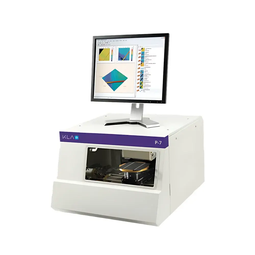
KLA P7 Stylus Profilometer
| Brand | KLA |
|---|---|
| Origin | Guangdong, China |
| Manufacturer Type | Authorized Distributor |
| Country of Origin | China |
| Model | P7 |
| Price | USD 70,000 (FOB Shenzhen) |
Overview
The KLA P7 Stylus Profilometer is a high-precision, benchtop surface metrology instrument engineered for quantitative topographic characterization of microstructured semiconductor wafers, thin-film stacks, MEMS devices, and advanced packaging substrates. Based on contact-mode mechanical profiling—where a diamond-tipped stylus traverses the sample surface under controlled normal force—the P7 implements proven scanning interferometry-coupled transduction architecture inherited from KLA’s industry-standard P-17 platform. It delivers traceable, NIST-compatible step height, roughness (Ra, Rq, Rz), warpage, and thin-film stress measurements with sub-nanometer vertical resolution and micron-level lateral repeatability. Designed for integration into front-end and back-end semiconductor process development labs, the P7 operates within Class 1000 cleanroom environments and supports wafer handling up to 150 mm diameter without image stitching—enabling full-die or full-wafer scan coverage in a single pass.
Key Features
- Benchtop form factor with vibration-isolated granite base and motorized Z-stage for stable, low-noise profiling
- Diamond stylus with 2 µm radius tip, selectable normal forces from 0.3–15 mg for soft film and hard substrate compatibility
- 150 mm maximum scan length in X-direction; 100 mm Y-travel for automated multi-site mapping
- Vertical resolution ≤ 0.1 nm (RMS) with 12-bit DAC feedback control and real-time thermal drift compensation
- Integrated auto-calibration routine using certified step-height standards (e.g., NIST SRM 2160)
- Modular software architecture supporting both standalone operation and SECS/GEM interface for factory automation
Sample Compatibility & Compliance
The P7 accommodates bare silicon, SOI, compound semiconductor (GaAs, SiC, GaN), glass, quartz, and polymer substrates ranging from 50 mm to 150 mm in diameter. Chuck vacuum ports support flatness-controlled clamping with ≤ 1 µm chuck-induced distortion. The system complies with SEMI E10 (Specification for Definition and Measurement of Equipment Reliability, Maintainability, and Availability), SEMI E11 (Equipment Communication Standard), and ISO/IEC 17025 requirements when operated under documented calibration and maintenance protocols. Measurement uncertainty budgets are traceable to national metrology institutes via KLA-certified calibration kits, and data audit trails satisfy GLP and internal QA documentation requirements per ISO 9001:2015 Clause 8.5.2.
Software & Data Management
KLA’s NanoMap™ v6.x software provides intuitive workflow-driven measurement sequencing, including automatic edge detection, multi-point leveling, and curvature correction algorithms for warpage analysis. All raw profilometry data—including analog voltage traces, filtered height maps, and statistical summaries—are stored in HDF5 format with embedded metadata (operator ID, timestamp, environmental conditions, calibration status). Software supports FDA 21 CFR Part 11-compliant electronic signatures, role-based access control, and encrypted database logging for GMP-regulated environments. Export options include CSV, DXF, STEP AP214, and native .nmf files compatible with KLA’s cross-platform analytics suite (e.g., YieldAnalyzer™ and ProcessWindow™).
Applications
- Quantitative verification of etch depth uniformity across 300 mm BEOL metal stack recess profiles
- Post-CMP dishing and erosion assessment on Cu/low-k interconnect test structures
- Thin-film stress mapping of PECVD SiNx layers on 200 mm Si wafers using Stoney equation integration
- Roughness validation of ALD HfO2 gate dielectrics per JEDEC JESD22-A121A
- MEMS cantilever deflection and release etch undercut metrology for inertial sensor qualification
- Wafer-level packaging (WLP) bump height and coplanarity analysis per IPC-7095C
FAQ
Is the P7 compatible with 200 mm and 300 mm wafers?
No—the P7 is optimized for wafers up to 150 mm (6-inch) diameter. For 200 mm and 300 mm applications, KLA recommends the P-17 or the next-generation P-15 series with extended travel stages.
Does the system support non-contact measurement modes?
No—the P7 is a dedicated stylus-based profilometer. Non-contact optical profiling (e.g., white-light interferometry) requires KLA’s optical platforms such as the eDR7 or RS-200 series.
What calibration standards are required for ISO/IEC 17025 compliance?
Certified step-height standards traceable to NIST (e.g., SRM 2160, SRM 1960) and roughness standards (e.g., VDI/VDE 2634 Part 2) must be used at defined intervals per your laboratory’s scope of accreditation.
Can the P7 export data directly to JMP or Python for statistical process control?
Yes—CSV and HDF5 exports contain fully annotated metrology data with SI-unit metadata, enabling direct ingestion into JMP, Minitab, Pandas, or custom SPC dashboards via KLA’s open API framework.


