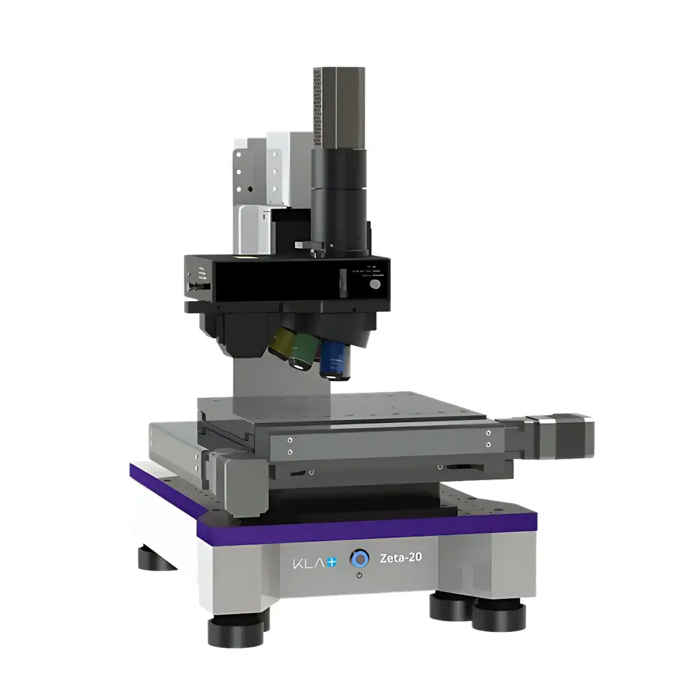
KLA Zeta20 Desktop Optical Profilometer
| Brand | KLA |
|---|---|
| Model | Zeta 20 |
| Origin | China (Guangdong) |
| Manufacturer Type | Authorized Distributor |
| Product Origin Classification | Domestic |
| Price | USD 98,000 (FOB Guangdong) |
| Measurement Principle | Multi-Mode Optical Interferometry & ZDot™ Confocal Imaging |
| Max. Vertical Range | >10 mm |
| Vertical Resolution | Sub-nanometer (typ.) |
| Lateral Resolution | ≤ 0.4 µm |
| Film Thickness Range | 1 nm – 50 µm (with integrated broadband reflectometry) |
| Sample Stage | Motorized XYZ with 100 mm × 100 mm travel |
| Software Platform | ZetaWare v6.x |
| Compliance | ISO 25178-2, ASTM E2981, SEMI S2/S8, GLP/GMP-ready audit trail |
Overview
The KLA Zeta20 Desktop Optical Profilometer is a high-precision, non-contact 3D surface metrology system engineered for quantitative topographic characterization across R&D laboratories and high-mix manufacturing environments. Unlike conventional laser scanning confocal microscopes, the Zeta20 implements a hybrid optical architecture combining ZDot™ proprietary confocal imaging with multi-modal interferometric techniques—including white light interferometry (WLI), Nomarski differential interference contrast (DIC), and shear interferometry—to deliver consistent, traceable measurements regardless of surface reflectivity, transparency, or texture. Its core measurement principle relies on real-time pixel-level focus evaluation across broadband illumination spectra, enabling simultaneous acquisition of nanoscale vertical profiles and diffraction-limited true-color extended-depth-of-field imagery. Designed to meet stringent requirements in semiconductor process development, MEMS packaging, advanced optics fabrication, and thin-film coating validation, the Zeta20 operates without sample charging, vacuum, or conductive coating—making it ideal for insulating, fragile, or temperature-sensitive substrates.
Key Features
- ZDot™ Confocal Mode: Captures high-fidelity 3D topography and full-spectrum true-color images in a single scan—no z-stack reconstruction required.
- Multi-Mode Optical Engine: Seamlessly switches between WLI (for smooth surfaces), DIC (for low-contrast features), and shear interferometry (for ultra-flat optics), optimizing signal-to-noise ratio per sample class.
- Broadband Reflectometry Integration: Measures film thickness from 1 nm to 50 µm on single- or multi-layer stacks using spectral reflectance modeling (e.g., Cauchy or Tauc-Lorentz dispersion models).
- Motorized Precision Stage: 100 mm × 100 mm XY travel with 0.1 µm repeatability and programmable Z-axis control supports automated wafer mapping and multi-site inspection routines.
- Robust Environmental Tolerance: Vibration-insensitive design with active focus stabilization enables operation on standard optical tables without active isolation.
- Modular Illumination: LED-based Köhler illumination with selectable wavelengths (405 nm–740 nm) ensures optimal contrast for transparent polymers, metal oxides, and patterned photoresists.
Sample Compatibility & Compliance
The Zeta20 accommodates samples ranging from bare silicon wafers and sapphire substrates to polymer films, glass optics, printed circuit boards, and biomedical scaffolds. It measures surfaces with reflectivity spanning 0.1%–100%, including highly transparent materials (e.g., fused silica, PDMS) and strongly scattering surfaces (e.g., sandblasted metals, anodized aluminum). All measurement modes are validated per ISO 25178-2 for areal surface texture parameters (Sa, Sq, Sz), ASTM E2981 for step height uncertainty quantification, and SEMI S2/S8 for equipment safety and ergonomics. The system’s software includes FDA 21 CFR Part 11-compliant user access controls, electronic signatures, and immutable audit trails—fully supporting GLP and GMP workflows in regulated industries.
Software & Data Management
ZetaWare v6.x provides a unified interface for instrument control, measurement automation, and metrology reporting. The platform supports custom script-driven recipes (Python API), batch processing of multi-wafer datasets, and direct export to industry-standard formats (STL, XYZ, CSV, TIFF, HDF5). Advanced analysis modules include ISO 13565-2 compliant roughness filtering, edge detection for critical dimension (CD) profiling, and multilayer film stack modeling with refractive index libraries. Raw data and processed results are stored in a relational database with time-stamped metadata, enabling full traceability from acquisition to certificate of conformance.
Applications
- Semiconductor: Quantifying etch depth uniformity, CMP planarity, and lithographic resist profile fidelity.
- MEMS & Sensors: Characterizing diaphragm deflection, comb-drive geometry, and hermetic seal integrity.
- Optics & Photonics: Measuring surface flatness of laser mirrors, wedge angles of prisms, and coating uniformity on AR/HR filters.
- Advanced Packaging: Validating underfill void distribution, solder bump height variation, and RDL line roughness.
- Materials Science: Correlating surface morphology with mechanical wear behavior, adhesion strength, or hydrophobicity.
- Quality Assurance: Automated defect classification (scratch, pit, particle) via machine-learning-enhanced image segmentation within ZetaWare.
FAQ
Does the Zeta20 require vacuum or conductive coating for non-conductive samples?
No. As a purely optical profilometer, it performs non-contact measurements on insulators, polymers, ceramics, and biological specimens without surface modification.
Can Zeta20 measure transparent thin films on transparent substrates?
Yes—integrated broadband reflectometry enables accurate thickness and optical constant extraction for single- and multi-layer stacks, including SiO₂ on fused silica or ITO on glass.
Is the system compatible with cleanroom Class 100 environments?
Yes. The Zeta20 meets SEMI S2 electrical safety standards and can be configured with static-dissipative enclosures and HEPA-filtered air purge options for Class 100/ISO 5 integration.
What calibration standards are supported?
NIST-traceable step height standards (e.g., NIST SRM 2160), roughness standards (e.g., ISO 25178 reference blocks), and film thickness standards (e.g., SiO₂/Si wafers with certified thickness) are fully supported.
How is measurement uncertainty reported?
ZetaWare calculates expanded uncertainty (k=2) per GUM (JCGM 100:2008) incorporating repeatability, environmental drift, stage positioning error, and optical model residuals—documented in each measurement report.


