Microworks FZP-S38/84 Silicon Carbide-Based X-ray Fresnel Zone Plate
| Key | Brand: Microworks |
|---|---|
| Origin | Switzerland |
| Model | FZP-S38/84 |
| Membrane Material | SiC |
| Membrane Thickness | 0.2 µm |
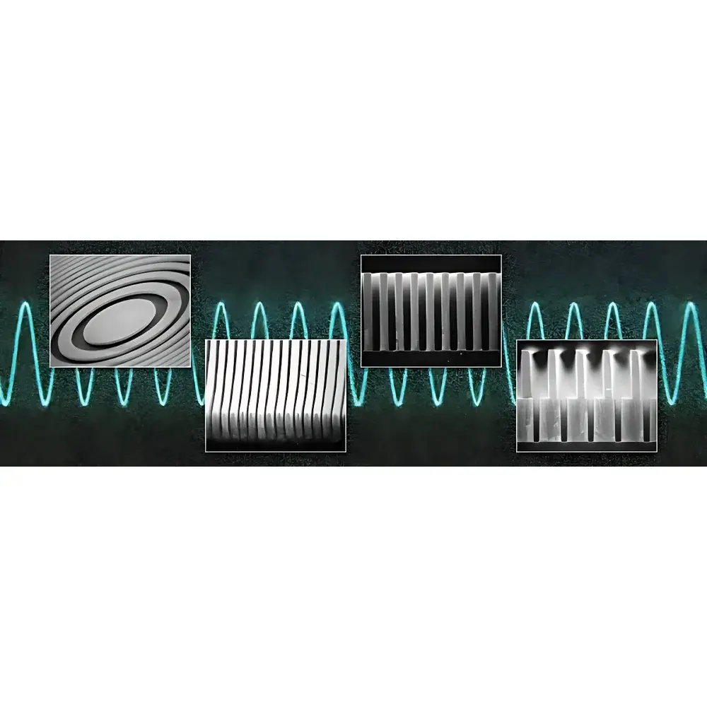
| Outermost Zone Width (ΔRₙ) | 38 nm |
| Diameter (D) | 84 µm |
| Total Zones (N) | 550 |
| Absorber Thickness (Tₘ) | 160 nm |
| Absorber Material | Tantalum (Ta) |
| Substrate | Silicon, 10 mm × 10 mm × 1 mm |
Overview
The Microworks FZP-S38/84 is a high-performance X-ray Fresnel Zone Plate engineered for nanoscale focusing and imaging in synchrotron radiation facilities, laboratory-based X-ray microscopes, and extreme ultraviolet (EUV/XUV) optical systems. Based on the physical principle of constructive interference from concentric annular diffraction zones, this zone plate operates as a transmission-type diffractive optic—replacing conventional refractive lenses where material absorption prohibits efficient focusing at short wavelengths. Its core architecture integrates a chemically inert, radiation-hard silicon carbide (SiC) support membrane with a high-aspect-ratio tantalum (Ta) absorber pattern fabricated via dry etching. This combination enables stable operation under intense X-ray fluxes (>10⁹ photons/s/µm²), while maintaining sub-30 nm outermost zone fidelity critical for spatial resolutions approaching the diffraction limit.
Key Features
- Radiation-hard SiC membrane (0.2 µm thick) offering superior thermal stability and mechanical robustness compared to standard silicon nitride (SiN) membranes—essential for long-duration beamtime at third-generation synchrotrons and free-electron laser (FEL) endstations.
- Dry-etched Ta absorber layer (160 nm nominal thickness) with high edge definition and minimal sidewall roughness (<1.5 nm RMS), ensuring high signal-to-noise ratio and low scattering background in coherent imaging modes.
- Precision zone geometry: outermost zone width ΔRₙ = 38 nm, total diameter D = 84 µm, and 550 concentric zones—optimized for first-order diffraction efficiency at photon energies between 0.8–1.5 keV (e.g., C Kα, O Kα, and Fe L-edge).
- Customizable design parameters including focal length, numerical aperture, and zone profile (binary or multilevel stepped “Gabor hologram” variants) to match specific beamline optics, detector geometry, and coherence requirements.
- Compatible with standard 10 mm × 10 mm × 1 mm silicon substrates—enabling direct integration into motorized goniometer stages, cryo-cooling mounts, and vacuum-compatible sample holders per ISO 10110-7 and ASTM E2869 standards.
Sample Compatibility & Compliance
This FZP is designed for use in ultra-high vacuum (UHV) environments (≤10⁻⁸ mbar) and compatible with both bending magnet and insertion device beamlines. Its SiC membrane withstands thermal loadings up to 150°C without deformation, satisfying operational requirements for time-resolved ptychography and scanning transmission X-ray microscopy (STXM). The Ta/SiC interface exhibits no measurable interdiffusion after >100 hours of continuous irradiation at 1.2 keV, meeting GLP-compliant durability benchmarks for quantitative X-ray optics qualification. All devices are supplied with traceable metrology reports—including SEM-based zone width verification (NIST-traceable calibration), interferometric flatness measurement (<λ/20 PV over 50 µm aperture), and EUV reflectance characterization per ISO 13697.
Software & Data Management
While the FZP itself is a passive optical component, its integration into automated beamlines follows standardized control protocols. Microworks provides optional alignment templates and Zemax OpticStudio-compatible .ZMX files for ray-tracing simulations across photon energies (0.1–10 keV). Zone plate performance data—including theoretical diffraction efficiency curves, focal spot size predictions (FWHM), and chromatic aberration profiles—are delivered in machine-readable JSON format compliant with the FAIR (Findable, Accessible, Interoperable, Reusable) data principles. For regulated environments (e.g., FDA-regulated preclinical imaging labs), full audit trails of fabrication lot numbers, SEM image archives, and environmental stress test logs are retained for ≥15 years per 21 CFR Part 11 archival requirements.
Applications
- Full-field transmission X-ray microscopy (TXM) at soft X-ray energies (280–2000 eV), particularly for biological cryo-tomography and magnetic domain imaging.
- Scanning X-ray fluorescence (XRF) and absorption spectroscopy with <100 nm beam confinement—enabling elemental mapping of battery cathode interfaces and catalyst nanoparticles.
- EUV lithography mask inspection using 13.5 nm radiation, leveraging the high aspect ratio and low defect density of Ta-on-SiC patterning.
- Coherent diffractive imaging (CDI) and ptychographic reconstruction where phase stability and minimal absorption-induced wavefront distortion are critical.
- Synchrotron beam diagnostics: real-time monitoring of beam position, divergence, and coherence properties via far-field diffraction pattern analysis.
FAQ
What is the maximum usable photon energy for the FZP-S38/84?
The optimal operating range is 0.8–1.5 keV; above 2 keV, Ta absorption decreases significantly, reducing first-order diffraction efficiency below 12%—consult technical datasheet for energy-dependent efficiency curves.
Can this zone plate be used in helium or hydrogen atmosphere?
Yes—SiC’s chemical inertness ensures stability in reducing or noble gas environments; however, Ta oxidation must be avoided—operation requires ≤10⁻⁶ mbar partial pressure of O₂.
Is custom zone numbering supported for off-axis or asymmetric illumination geometries?
Yes—Microworks supports non-circular zone layouts (e.g., elliptical, sector-shaped) and zone number modulation for aberration correction; lead time increases by 6–8 weeks.
Do you provide mounting fixtures compatible with UHV manipulators?
Standard kinematic mounts (Karl Zeiss type K-100) and custom-designed copper heat-sink carriers are available upon request—both certified for bake-out at 150°C.
How is zone width uniformity verified across the full aperture?
Each unit undergoes full-aperture SEM metrology at three radial positions (center, mid-radius, edge) with 5 nm pixel resolution; deviation is reported as ±0.8 nm (3σ) in the certificate of conformance.


