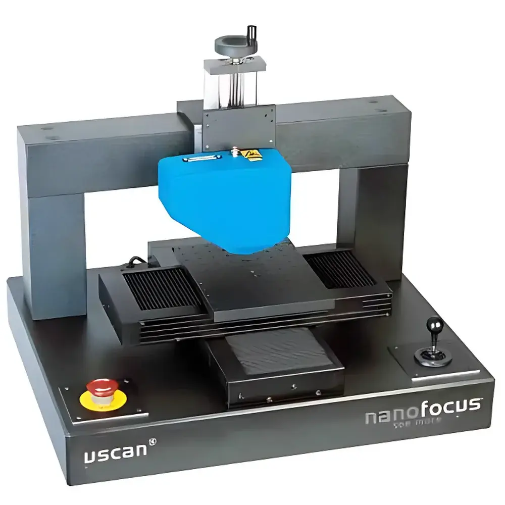
NanoFocus μScan Non-Contact Laser Scanning Profilometer
| Origin | Germany |
|---|---|
| Manufacturer Type | Authorized Distributor |
| Origin Category | Imported |
| Model | NanoFocus μScan |
| Product Type | Non-Contact Profilometer / Surface Roughness Analyzer |
| Scan Modules | SC 50 (50×50 mm XY range, 0.5 µm XY resolution, 100 mm Z positioning, 50 mm/s max speed) |
| Z-Sensors | Confocal Point (CF 4: 0.02 µm Z res, 1 µm XY res, 4 mm WD, 1.0 mm Z range |
| CF 13 | same Z res, 13 mm WD) |
| Autofocus (AF 2 | 0.025/0.011 µm Z res, 2 mm Z range, dual WD modes) |
| Chromatic White Light (CRT 5 | 0.010 µm Z res, 4 µm XY res, 5 mm Z range, 0.3 mm WD) |
| Holographic (CP 15 | 3.0 µm Z res, 12 µm XY res, 12 mm Z range) |
| System Controller | Industrial PC with Windows XP Professional, DVD writer, Ethernet |
| Mechanical Platforms | MT 70 cabinet (1550×800×750 mm), MP 100 granite stand (660×450×497 mm) for SC 50–SC 150, MP 200 (680×480×385 mm) for SC 200 |
| Software | NF μsoft (DIN EN ISO-compliant roughness analysis, profile & topography rendering), NF 3D-Plus (OpenGL-based photorealistic 3D visualization), NF ActiveX (VBA/Excel integration), NF Hybridmaster (SMT thick-film SPC & teach-in), NF Flatmaster (flatness/warpage automation), NF Solder (offline solder paste inspection), NF AutoScan (arbitrary-point profiling) |
Overview
The NanoFocus μScan is a high-precision, non-contact laser scanning profilometer engineered for traceable, sub-micrometer topographic characterization of technical surfaces. It operates on the principle of active optical triangulation combined with sensor-specific depth-sensing mechanisms—including confocal laser scanning, chromatic aberration-based white-light interferometry, autofocus feedback control, and holographic reconstruction—to deliver calibrated height data across diverse material classes and surface geometries. Designed for integration into industrial metrology workflows, the system meets foundational requirements for geometric measurement traceability under ISO/IEC 17025 and supports compliance-critical applications in semiconductor packaging, microelectronics assembly, and precision mechanical manufacturing. Its modular architecture decouples XY scanning motion (via motorized stages) from Z-axis sensing—enabling flexible configuration for varying field-of-view, resolution, and working distance constraints without mechanical compromise.
Key Features
- Modular scan platform architecture: Interchangeable SC-series scanning modules (SC 50 to SC 200) provide XY measurement fields from 50×50 mm to 200×200 mm, all with uniform 0.5 µm positional resolution and 100 mm Z-axis travel.
- Multi-sensor compatibility: Supports four distinct Z-height sensing technologies—confocal point sensors (CF 4, CF 13), autofocus sensors (AF 2, AF 5), chromatic white-light sensors (CRT 5, CRT 12, CRT 16), and holographic sensors (CP 15, CP 42, CP 65)—each optimized for specific surface reflectivity, slope, and roughness regimes.
- Sub-10 nm vertical resolution capability: Achieved via high-stability optical paths, temperature-compensated granite metrology bases (MP 100/MP 200), and vibration-damped MT 70 system cabinets compliant with ISO 10360-2 environmental specifications.
- Industrial-grade controller: Embedded high-performance PC running Windows XP Professional with real-time motion control, network connectivity, and native support for automated script execution via NF ActiveX interface.
- Calibration-ready design: All sensors include documented calibration certificates traceable to PTB (Physikalisch-Technische Bundesanstalt) standards; software implements DIN EN ISO 4287, ISO 25178, and ASME B46.1 roughness and areal parameter algorithms.
Sample Compatibility & Compliance
The μScan accommodates reflective, translucent, and moderately absorptive surfaces—including silicon wafers, ceramic substrates, metal stampings, polymer films, and solder paste deposits—without risk of thermal loading or mechanical deformation. Its non-contact operation eliminates stylus wear and avoids contamination of sensitive microstructures. The system conforms to electromagnetic compatibility (EMC) Directive 2014/30/EU and Low Voltage Directive 2014/35/EU. Software modules such as NF Hybridmaster and NF Solder support statistical process control (SPC) data logging aligned with IATF 16949 and IPC-A-610 requirements. Audit trails, user access controls, and electronic signature capabilities in NF μsoft satisfy documentation integrity expectations under FDA 21 CFR Part 11 for regulated environments.
Software & Data Management
NF μsoft serves as the unified control and evaluation environment, delivering full-profile acquisition, cross-sectional analysis, and areal topography reconstruction. Roughness parameters—including Sa, Sq, Sz, Sk, Spk, and Svk—are calculated per DIN EN ISO 25178-2 and exported in CSV, TXT, or proprietary .nfs formats. NF 3D-Plus enables photorealistic OpenGL rendering with adjustable lighting, transparency, and false-color mapping for rapid defect localization. NF ActiveX permits programmatic integration with Excel/VBA, LabVIEW, or custom MES platforms for batch measurement sequencing and inline reporting. Optional modules like NF Flatmaster execute fully automated flatness deviation analysis over rectangular or circular domains using least-squares fitting per ISO 1101; NF AutoScan supports coordinate-driven measurement point definition via external CAD import (IGES, STEP).
Applications
- Semiconductor packaging: Warpage measurement of leadframes and molded IC packages; bump height and coplanarity verification post-reflow.
- SMT production control: Offline volumetric assessment of solder paste deposition (area, volume, height, bridge detection) per IPC-7530 guidelines.
- Thick-film hybrid circuitry: Automated thickness mapping of screen-printed resistive and conductive layers across alumina or beryllia substrates.
- Precision optics and MEMS: Characterization of micro-lens arrays, diffractive optical elements, and actuator surface profiles with sub-micron form error quantification.
- Medical device manufacturing: Surface texture validation of laser-textured orthopedic implants and microfluidic channel geometry verification.
FAQ
What surface roughness parameters does the μScan calculate in compliance with international standards?
NF μsoft computes all primary areal and profile-based parameters defined in DIN EN ISO 25178-2 and ISO 4287, including Sa, Sq, Sz, Ssk, Sku, Sds, Sal, Str, and functional parameters such as Smr, Vmp, Vmc, and Vvv.
Can the system be integrated into an automated production line?
Yes—via NF ActiveX, NF Hybridmaster, and programmable I/O interfaces, the μScan supports trigger-based measurement initiation, pass/fail decision output, and real-time SPC charting compatible with factory-level SCADA and MES infrastructure.
Is calibration documentation provided with each sensor module?
Each delivered sensor carries a manufacturer-issued calibration certificate traceable to national metrology institutes (e.g., PTB), including uncertainty budgets and verification of linearity, repeatability, and thermal drift performance.
What is the maximum allowable surface slope for reliable measurement with the CRT 5 chromatic sensor?
The CRT 5 sensor maintains valid height data acquisition up to ±12° local surface inclination under standard illumination conditions; steeper slopes require tilt compensation via multi-angle acquisition or sensor reorientation.
Does the system support GLP/GMP audit requirements for pharmaceutical or medical device labs?
NF μsoft includes configurable electronic signatures, time-stamped audit logs, role-based access control, and 21 CFR Part 11–compliant data integrity features when deployed with validated installation and operational qualification protocols.