Nanoimprint Resist Series IPNR – Advanced Functional Polymer Materials for Semiconductor Nano-Patterning
No specifications available.
Overview
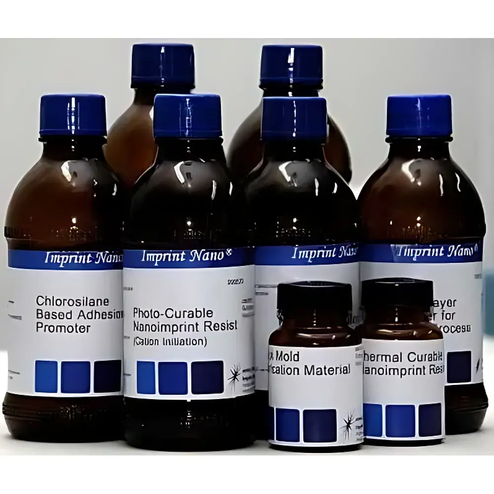
The IPNR Nanoimprint Resist Series is a comprehensive portfolio of high-performance, application-specific polymer formulations engineered for thermal and photo-based nanoimprint lithography (NIL) processes in advanced semiconductor manufacturing, MEMS fabrication, and nanophotonic device development. Unlike generic photoresists, IPNR materials are chemically tailored to meet the stringent requirements of sub-20 nm pattern fidelity, low residual layer thickness (RLT), high etch selectivity, and interfacial stability across diverse stamp–substrate interfaces. Each formulation operates on well-established physical principles: thermoplastic variants (IPNR-T1000) rely on reversible glass transition-driven flow under controlled temperature and pressure; thermoset types (IPNR-T2000) undergo covalent network formation via thermally activated crosslinking; while photopolymerizable resists (IPNR-PC1000/PC2000) exploit either free-radical or cationic photoinitiation pathways under UV exposure—enabling precise spatial control over polymerization kinetics and final mechanical robustness. The series supports both rigid quartz/metal stamps and flexible PDMS molds, and is validated for compatibility with industry-standard NIL platforms including Obducat Eitre, SUSS MicroTec MA/BA series, EVG620/720 systems, and HP’s proprietary nanoimprint tools.
Key Features
- Multi-mechanism resist platform: Thermoplastic (T1000), thermosetting (T2000), free-radical (PC1000), and cationic (PC2000) photopolymerization chemistries — enabling process flexibility across thermal, UV, and hybrid imprint schemes.
- Dedicated underlayer engineering: IPNR-UL1000 provides clean lift-off capability with controlled solubility contrast; IPNR-UL2000 delivers high plasma etch resistance (>8:1 SiO₂ selectivity) as an etch mask for subsequent pattern transfer.
- Template interface optimization: IPNR-AP chlorosilane-based adhesion promoter enhances covalent bonding to Si/SiO₂ wafers; complementary anti-sticking agents (custom-formulated per mold material) minimize defect generation and enable >100-cycle mold lifetime.
- Rapid prototyping support: IPNR-UPM enables direct, maskless fabrication of low-cost, high-fidelity quartz or silicon master templates via spin-coating and reactive ion etching—reducing time-to-pattern from weeks to hours.
- Batch-to-batch reproducibility: All formulations are manufactured under ISO 9001-certified cleanroom conditions (Class 1000), with QC verification of viscosity (Brookfield DV2T), gel content (FTIR), and film uniformity (ellipsometry).
Sample Compatibility & Compliance
IPNR resists are qualified for use on standard 100–300 mm semiconductor wafers (Si, SiO₂, SiN, GaAs, InP, fused silica), as well as flexible substrates (PET, PI, quartz). All materials comply with SEMI S2-0215 safety guidelines and are supplied with full SDS documentation. Resists are compatible with standard cleanroom processing environments (ISO Class 5–6) and support GLP-aligned process documentation workflows. While not pre-certified to specific FDA or IEC standards (as they are non-device materials), their chemical composition excludes REACH SVHC-listed substances and meets RoHS Directive 2011/65/EU requirements. Trace metal impurity profiles (<1 ppb Fe, Cr, Ni) are verified by ICP-MS for front-end-of-line (FEOL) integration.
Software & Data Management
As consumable polymer materials, IPNR products do not incorporate embedded firmware or software. However, their performance is fully integrable into automated NIL process control systems via standardized recipe frameworks (SEMI E30/GEM). Process parameters—including spin speed (500–6000 rpm), soft-bake profile (80–180 °C, 60–120 s), imprint temperature/pressure (for thermal variants), and UV dose (100–1500 mJ/cm², 365 nm) — are documented in machine-readable format (CSV/XML) and supported by manufacturer-provided process integration guides. Audit trails for material lot traceability, expiration tracking, and environmental storage logs (temperature/humidity) can be maintained within existing MES platforms compliant with ISO 13485 or FDA 21 CFR Part 11 when used in regulated R&D or pilot-line environments.
Applications
- High-resolution patterning for EUV mask repair templates and diffractive optical elements (DOEs)
- Sub-10 nm line/space definition in plasmonic metasurfaces and photonic crystal slabs
- Low-defect-area fabrication of nanostructured anti-reflective coatings (ARCs) for imaging sensors
- Direct-write functionalization of bio-sensing surfaces using lift-off-defined electrode arrays
- Hybrid lithography integration: IPNR-PC2000 serves dual role as NIL resist and i-line stepper-compatible photoresist (λ = 365 nm), enabling seamless overlay alignment in multi-layer stack processing.
FAQ
Are IPNR resists compatible with roll-to-roll (R2R) nanoimprint systems?
Yes — IPNR-T1000 and IPNR-PC1000 have been successfully deployed in pilot-scale R2R NIL tools operating at web speeds up to 0.5 m/min; viscosity and drying kinetics are optimized for continuous coating and flash-cure integration.
Can IPNR-UL2000 withstand chlorine-based ICP etching for GaN device fabrication?
Yes — IPNR-UL2000 exhibits >92% thickness retention after 120 s Cl₂/BCl₃ ICP etch (100 W, 5 mTorr), making it suitable for GaN HEMT gate recess and LED mesa isolation.
Is lot-level certification data provided with each shipment?
Yes — each batch includes a Certificate of Analysis (CoA) listing viscosity (mPa·s @ 25 °C), solids content (wt%), and residual solvent concentration (GC-FID), traceable to NIST-calibrated instrumentation.
Do you offer custom formulation development for proprietary template chemistries?
Yes — our technical team collaborates with customers under NDA to tailor surface energy, Tg, or etch resistance profiles, with typical lead time of 8–12 weeks for qualification-grade samples.


