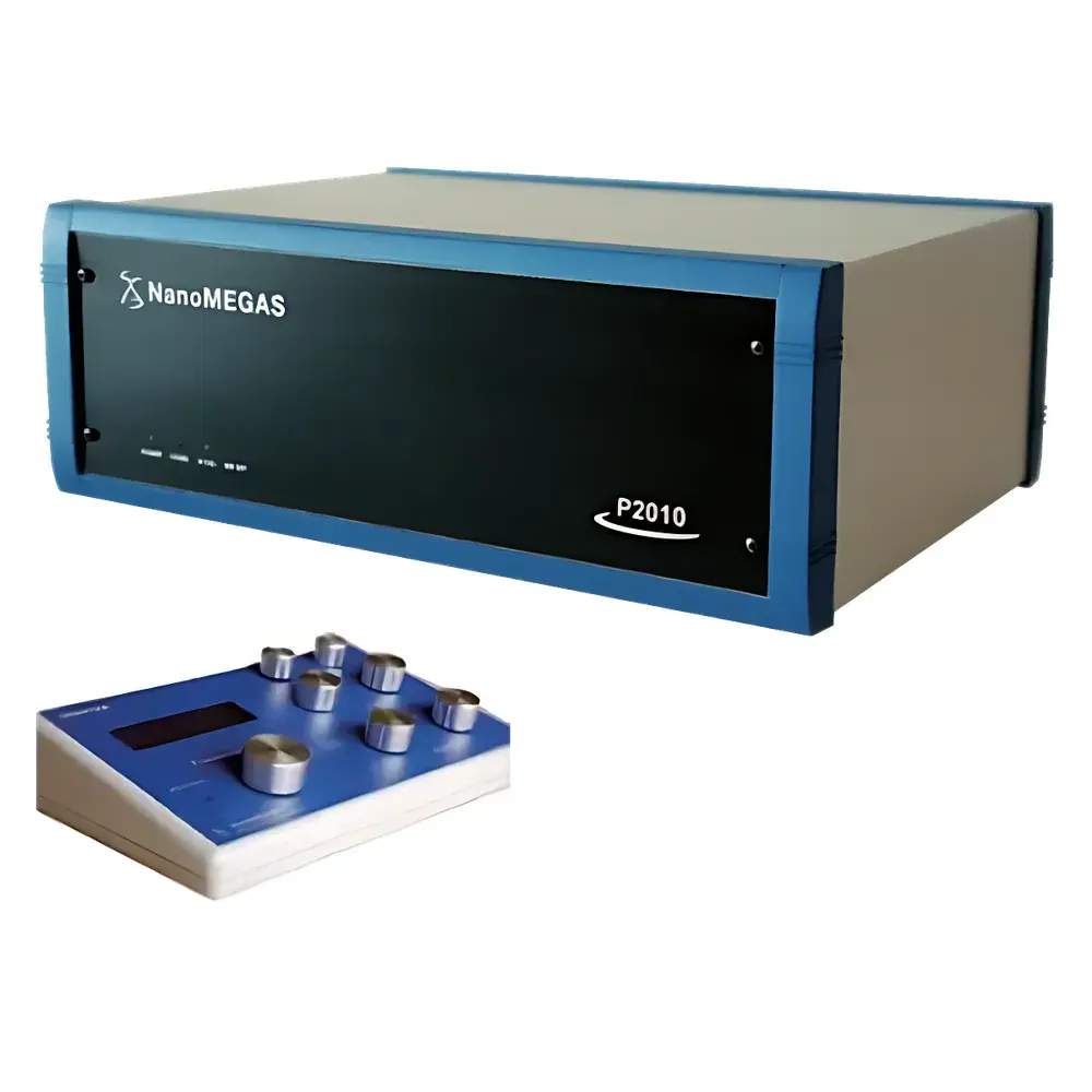
NanoMEGAS DigiSTAR Precession Electron Diffraction and Nanocrystal Analysis System
| Brand | NanoMEGAS |
|---|---|
| Origin | Imported (Non-China) |
| Manufacturer Type | Authorized Distributor |
| Model | DigiSTAR |
| Pricing | Upon Request |
Overview
The NanoMEGAS DigiSTAR Precession Electron Diffraction (PED) and Nanocrystal Analysis System is a modular, high-precision instrumentation platform engineered for quantitative microstructural characterization in transmission electron microscopy (TEM). It enables robust acquisition and interpretation of precessed electron diffraction patterns—leveraging the fundamental principle of controlled beam precession to suppress dynamical diffraction effects and enhance kinematical approximation. This significantly improves pattern interpretability, indexing reliability, and crystallographic fidelity compared to conventional selected-area electron diffraction (SAED) or nanobeam electron diffraction (NBD). Designed for integration with 200–300 kV TEMs equipped with field-emission guns (FEG), DigiSTAR operates independently of STEM hardware, supporting both TEM and STEM imaging modes without requiring dedicated scanning coils or detector synchronization. Its core architecture comprises three tightly coupled software modules—TopSPIN, ASTAR, and STRAIN—alongside the ADT-3D reconstruction suite, collectively enabling comprehensive orientation mapping, phase identification, strain quantification, and 3D reciprocal-space modeling at nanometer-scale spatial resolution.
Key Features
- Hardware-agnostic PED control: Fully functional on TEMs with or without integrated STEM capabilities; no dependency on manufacturer-specific scanning hardware.
- Precise beam precession: Adjustable precession angle range from 0° to 2.5°; precession frequency up to ≥300 Hz when paired with Merlin 1R direct electron detector (subject to TEM stability and column performance).
- Nanometer-scale probe control: Minimum probe size ≤2 nm under FEG-TEM conditions; supports both parallel-beam and nanoprobe illumination modes.
- Independent beam alignment and de-scanning: Real-time, decoupled adjustment of beam tilt, centering, and precession axis during acquisition—ensuring optimal pattern symmetry and minimal dynamical artifacts.
- Zero-impact mode switching: Disabling the precession controller restores native TEM operation without altering lens excitations, stigmator settings, or beam alignment parameters.
- Modular software integration: Seamless interoperability between TopSPIN (acquisition), ASTAR (orientation/phase mapping), STRAIN (lattice distortion analysis), and ADT-3D (3D reciprocal-space reconstruction).
Sample Compatibility & Compliance
DigiSTAR is compatible with standard TEM specimen geometries (3 mm diameter, <100 nm thick) across metallic alloys (e.g., Ti, Al-based systems), semiconductor heterostructures (e.g., Si/SiGe multilayers), and ceramic nanocomposites (e.g., TiN/Al bilayers). All software modules comply with GLP-aligned data integrity requirements: TopSPIN enforces audit-trail logging of acquisition parameters (precession angle, dwell time, step size, detector gain); ASTAR and STRAIN preserve raw pattern metadata—including camera constant, pixel size, and calibration timestamps—for traceable post-processing. While not certified to FDA 21 CFR Part 11 by default, the system supports export of FAIR-compliant HDF5 datasets and can be configured within validated laboratory environments per ISO/IEC 17025 or ASTM E2962–22 (Standard Guide for Electron Backscatter Diffraction Analysis) guidelines.
Software & Data Management
TopSPIN provides synchronized control of beam precession, stage movement, and detector readout—supporting point, line, and area scans with sub-nanometer step resolution (≤1 nm). It delivers virtual bright-field/dark-field imaging via real-time pattern integration and includes gamma correction, histogram normalization, and automated TIFF/PNG export. ASTAR performs fully automated indexing using dynamically generated templates covering all 7 crystal systems; outputs include orientation distribution maps (ODFs), phase maps, grain boundary networks (with Σ-value classification), and twin identification. STRAIN computes lattice parameter deviations from reference patterns with ≤±0.02% relative strain precision and ≤3 nm spatial resolution. ADT-3D reconstructs 3D reciprocal lattices from tilt-series PED data (±40° tilt range, 1° increments), extracting unit-cell parameters with ~2–3% accuracy and enabling structure solution workflows compatible with external crystallographic packages (e.g., JANA, SHELX).
Applications
DigiSTAR is routinely deployed in advanced materials R&D for: (1) Quantitative phase fraction analysis in multiphase alloys (e.g., α/β Ti-6Al-4V); (2) Interface-resolved orientation mapping in epitaxial multilayers (e.g., Al/TiN stacks); (3) Strain gradient profiling across quantum-well heterojunctions (e.g., Si/SiGe); (4) Defect-sensitive crystallographic analysis of dislocation cores and stacking faults; (5) Ab initio structure determination of nano-crystalline or beam-sensitive phases where XRD fails. Its ability to operate under low-dose conditions—particularly with Merlin 1R’s high DQE—makes it suitable for radiation-sensitive organic-inorganic hybrids and battery electrode materials.
FAQ
Does DigiSTAR require a dedicated STEM column or scanning coils?
No. DigiSTAR generates beam precession electromagnetically via its own deflector system and does not rely on the TEM’s scanning hardware.
Can ASTAR index unknown crystal structures without prior knowledge?
ASTAR requires a crystallographic model (unit cell + space group) for template matching; however, ADT-3D output can be exported to external crystallography software for ab initio structure solution.
Is real-time drift correction available during PED acquisition?
Yes—TopSPIN implements frame-by-frame cross-correlation-based drift compensation during series acquisition.
What detector types are supported?
Full compatibility with Gatan K2/K3, FEI Ceta, and Quantum Detectors Merlin 1R; camera constant calibration is assisted via built-in polycrystalline Au or Si standards.
Can STRAIN quantify elastic strain in amorphous/crystalline interfaces?
STRAIN operates exclusively on indexed crystalline regions; amorphous zones are masked automatically during strain tensor calculation.


