NanoMEGAS TopSPIN STRAIN: TEM Strain Analysis Software for Precession Electron Diffraction
| Brand | NanoMEGAS |
|---|---|
| Origin | Belgium |
| Model | TopSPIN STRAIN |
| Application | Automated High-Resolution Strain Mapping in Scanning Transmission Electron Microscopy (STEM) using 4D Scanning Precession Electron Diffraction (4D-SPED) |
| Spatial Resolution | 2–3 nm (FEG-TEM) |
| Strain Sensitivity | < 2 × 10⁻⁴ |
| Typical Acquisition Time | 5–10 min (150 × 150 pixels) |
| Pixel Dwell Time | 10–40 ms |
| Strain Quantification Accuracy | ±0.02% (at 200 kV FEG-TEM) |
| Analysis Engine | AppFive proprietary algorithm |
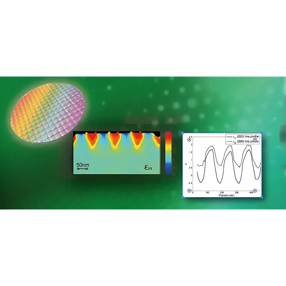
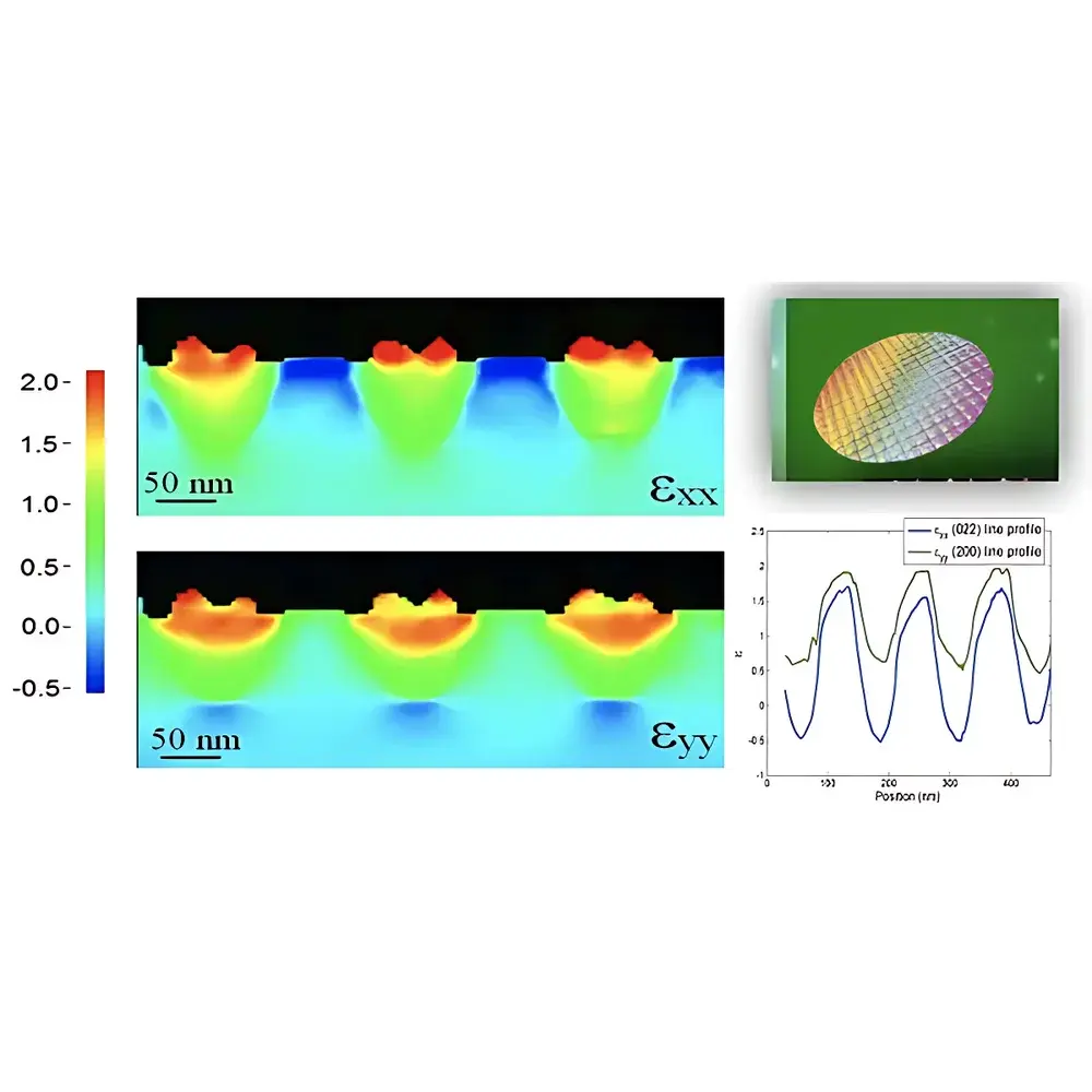
| Output Modalities | Point, line, and 2D strain tensor maps (εₓₓ, ε_zz, ε_xz), orientation/phase/strain/STEM co-registration |
Overview
NanoMEGAS TopSPIN STRAIN is a dedicated software platform engineered for quantitative, high-spatial-resolution strain mapping in scanning transmission electron microscopy (STEM) via 4D scanning precession electron diffraction (4D-SPED). It implements a physically grounded approach to lattice distortion analysis by leveraging the angular stability and intensity fidelity of precessed electron diffraction patterns acquired pixel-by-pixel across a defined scan area. Unlike conventional geometric phase analysis (GPA) or digital image correlation (DIC)-based methods applied to high-angle annular dark-field (HAADF) images, TopSPIN STRAIN operates directly on the reciprocal-space information encoded in diffraction disks—enabling robust strain quantification independent of sample thickness gradients, beam-induced drift, or imaging artifacts. The solution is specifically optimized for advanced semiconductor metrology, including strain engineering validation in sub-10 nm MOSFET architectures, heteroepitaxial interface characterization, and nanoscale stressor integration assessment in SiGe, GaN, and 2D material systems.
Key Features
- Full integration with NanoMEGAS SPINNING® hardware for synchronized beam precession control and pattern acquisition during STEM raster scanning
- Automated strain tensor reconstruction (εxx, εyy, εzz, εxz, etc.) from 4D-SPED datasets using the AppFive algorithm—validated against finite element modeling and X-ray microdiffraction benchmarks
- Sub-nanometer spatial registration between strain maps and simultaneously acquired HAADF-STEM reference images, virtual bright-field (VBF) images, and phase/orientation maps
- Real-time feedback on diffraction pattern quality (disk sharpness, signal-to-noise ratio, precession angle consistency) during acquisition to ensure data integrity
- Batch processing capability for multi-region analysis across multiple samples, supporting standardized reporting formats compliant with internal QA workflows
- Native support for NIST-traceable calibration standards and user-defined lattice parameter references (e.g., unstrained Si, Ge, or AlN templates)
Sample Compatibility & Compliance
TopSPIN STRAIN is compatible with standard FEG-TEM/STEM platforms operating at 80–300 kV, including JEOL ARM series, Thermo Fisher Scientific Titan and Talos systems, and Hitachi HT7800/HT7900. It accepts raw 4D-SPED data in HDF5, MRC, or EM format, preserving full metadata (scan parameters, camera length, precession angle, convergence angle). The software adheres to GLP-aligned documentation practices: all processing steps—including background subtraction, disk centering, reference lattice assignment, and strain interpolation—are logged with timestamps and operator identifiers. While not certified under FDA 21 CFR Part 11, its audit trail functionality supports internal validation protocols required for ISO/IEC 17025-accredited laboratories and semiconductor process development environments governed by ITRS roadmap guidelines.
Software & Data Management
Data handling follows FAIR principles (Findable, Accessible, Interoperable, Reusable). Processed strain maps are exported as 16-bit TIFF stacks with embedded scale bars and metadata headers compliant with EMDB and MRC conventions. ASCII-based strain profile exports (X, Y, εxx, εzz, εxz, σxx, etc.) enable direct import into MATLAB, Python (NumPy/Pandas), or commercial statistical packages for multivariate correlation analysis. Version-controlled configuration files (.topspin) allow replication of analysis pipelines across instruments and sites. No cloud connectivity or remote telemetry is enabled by default; all computation occurs locally on the host workstation, ensuring compliance with corporate IT security policies governing sensitive process IP.
Applications
- Quantitative validation of strain transfer efficiency from SiN stressors to Si channel regions in nMOS/pMOS devices
- Strain relaxation profiling across graded SiGe buffer layers and quantum well interfaces
- Local elastic strain mapping in freestanding Ge microdisks, nanowires, and van der Waals heterostructures
- Correlative strain–defect analysis: overlaying dislocation core positions (from GPA or deep learning segmentation) onto εij fields to assess strain shielding effects
- Process window optimization for selective epitaxy, atomic layer deposition (ALD) capping, and rapid thermal annealing (RTA) cycles
FAQ
What electron optics configurations are required to achieve 2–3 nm spatial resolution?
Optimal performance requires a monochromated FEG source, probe-forming aperture ≤30 µm, and convergence semi-angle ≥25 mrad. Probe current should be maintained between 50–200 pA to balance diffraction signal strength and radiation damage in beam-sensitive materials.
Can TopSPIN STRAIN analyze polycrystalline or textured thin films?
Yes—provided individual grains yield sufficiently distinct diffraction signatures. Grain boundary strain mapping is supported via automated grain segmentation integrated with orientation mapping modules in TOPSPIN Suite.
Is calibration against a known standard mandatory before each session?
While not strictly mandatory, NanoMEGAS recommends daily calibration using a certified Si [001] or Au standard to correct for minor drift in camera length and detector tilt—particularly critical when comparing datasets acquired across different instrument sessions or operators.
Does the software support dynamic in-situ strain measurements?
Not in real time; however, sequential 4D-SPED acquisitions (e.g., under heating or biasing) can be processed retrospectively to generate time-resolved strain evolution series, provided mechanical and thermal drift are compensated via fiducial tracking.
How is uncertainty propagated through the AppFive algorithm?
Uncertainty estimation is based on Poisson statistics of detected electrons per diffraction disk, combined with Monte Carlo simulation of lattice parameter fitting residuals. Per-pixel relative uncertainty in εxx is reported alongside the primary map and typically falls within ±0.005% to ±0.03% depending on local SNR and pattern quality.


