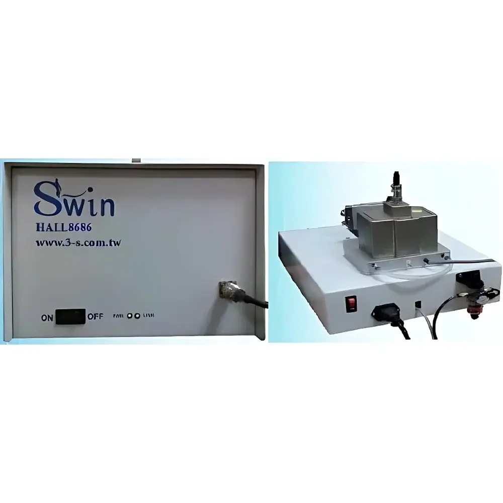
Oelabs Hall8686 Variable-Temperature Hall Effect Measurement System
| Brand | Oelabs |
|---|---|
| Origin | Taiwan |
| Model | Hall8686 |
| Magnetic Field Strength | 0.53 T |
| Temperature Range | 77 K–423 K (optional up to 623 K) |
| Temperature Accuracy | ±0.5 K |
| Current Output | 1 nA–100 mA |
| Voltage Resolution | down to nV level (up to 300 V) |
| Carrier Concentration Range | 10⁷–10²¹ cm⁻³ |
| Mobility Range | 1–10⁷ cm²/(V·s) |
| Resistivity Range | 10⁻⁵–10⁷ Ω·cm |
| Sample Size | 5–15 mm diameter, thickness ≤1 mm |
| Sample Holder | proprietary spring-loaded four-point probe fixture |
| Compatible Materials | Si, ZnO, SiGe, SiC, GaAs, InGaAs, InP, GaN (n-type and p-type) |
Overview
The Oelabs Hall8686 Variable-Temperature Hall Effect Measurement System is a precision-engineered instrument designed for quantitative characterization of charge transport properties in semiconductor materials under controlled thermal conditions. Based on the Van der Pauw method and classical Hall effect theory, the system measures key electronic parameters—including bulk and sheet carrier concentration, Hall mobility, resistivity, and Hall coefficient—across a wide temperature range (77 K to 423 K, extendable to 623 K). Its integrated cryogenic and heating capabilities enable thermally activated transport analysis, defect-state mapping, and band-structure-related parameter extraction. The system is widely deployed in academic research laboratories, national institutes, and semiconductor R&D facilities where reproducible, traceable, and standards-compliant Hall measurements are required for process development, epitaxial layer qualification (e.g., LED epi-wafers), HEMT 2DEG verification, and photovoltaic cell process monitoring.
Key Features
- Ultra-low-noise current source with 1 nA minimum resolution—enabling reliable measurement of semi-insulating and high-resistivity materials (up to 10⁷ Ω·cm).
- High-sensitivity nanovolt-level voltage measurement (down to nV resolution, up to 300 V range), optimized for low-resistance samples and Ohmic contact validation.
- Integrated temperature-controlled stage with ±0.5 K accuracy over 77–423 K; optional high-temperature extension to 623 K using resistive heating and PID-regulated feedback.
- Proprietary spring-loaded four-point probe fixture eliminates the need for lithographic Hall bar patterning—supporting rapid, non-destructive evaluation of as-grown wafers and bulk crystals (5–15 mm diameter, ≤1 mm thick).
- Real-time I–V curve acquisition across all probe configurations (ABCD) for immediate assessment of contact linearity and Ohmic behavior prior to Hall analysis.
- Single-interface software environment: all instrument control, data acquisition, Van der Pauw correction, and parameter calculation (nB, nS, μ, ρ, RH) occur within one unified GUI—no manual switching or post-processing required.
Sample Compatibility & Compliance
The Hall8686 supports direct electrical characterization of both bulk and thin-film semiconductor materials without sample fabrication. Validated substrates include Si, SiC, GaN, GaAs, InP, InGaAs, ZnO, and SiGe—covering n-type and p-type doping regimes across nine orders of magnitude in carrier concentration (10⁷–10²¹ cm⁻³) and seven decades in resistivity (10⁻⁵–10⁷ Ω·cm). The system adheres to ASTM F76–22 (“Standard Test Method for Measuring Resistivity and Hall Coefficient of Semiconductor Materials Using the Van der Pauw Technique”) and supports GLP-compliant operation through timestamped audit logs, user-access controls, and raw-data export in CSV and HDF5 formats. Optional 21 CFR Part 11–ready software modules provide electronic signatures, change tracking, and secure data archiving for regulated environments.
Software & Data Management
Oelabs’ proprietary HallControl™ software provides real-time visualization of temperature ramp profiles, magnetic field stability, current/voltage traces, and calculated transport parameters. All measurements are time-stamped and metadata-tagged (operator ID, sample ID, ambient pressure, cooling gas flow rate if applicable). Export functions support ISO/IEC 17025–aligned reporting templates, including uncertainty propagation estimates based on instrument specifications and Van der Pauw geometric correction factors. Batch processing mode enables automated multi-sample sequences with configurable dwell times and thermal soak protocols. Raw voltage/current datasets are stored in open-format HDF5 files—ensuring long-term readability and compatibility with Python (NumPy, SciPy), MATLAB, and OriginLab workflows.
Applications
- Quantitative evaluation of dopant activation efficiency and ion implantation annealing in Si and compound semiconductors.
- Epitaxial layer quality screening for LED manufacturing—correlating Hall mobility and carrier concentration with luminescence efficiency and defect density.
- Verification of two-dimensional electron gas (2DEG) formation and sheet density stability in AlGaN/GaN HEMT heterostructures.
- Thermally activated conduction analysis in perovskite and organic photovoltaic absorbers—extracting activation energies and trap-state distributions.
- Process control in SiC power device fabrication—monitoring drift layer resistivity uniformity and compensation effects across wafers.
- Fundamental research on topological insulators and narrow-bandgap semiconductors requiring low-temperature (<100 K) transport characterization.
FAQ
What temperature calibration standard does the Hall8686 use?
The system employs calibrated Pt-100 sensors traceable to NIST standards, with factory verification at liquid nitrogen (77 K), room temperature (295 K), and 400 K. Users may perform in-situ recalibration using certified reference materials.
Can the Hall8686 measure anisotropic or layered materials?
Yes—the Van der Pauw geometry inherently assumes isotropic conductivity, but the instrument supports rotational sample mounting (optional add-on) and multi-angle magnetic field alignment for preliminary anisotropy screening. For rigorous tensor analysis, complementary magnetotransport modules are available.
Is the spring probe fixture compatible with fragile or patterned wafers?
The probe force is mechanically limited to <0.5 N per tip and fully adjustable; soft-contact mode is recommended for MEMS devices or oxide-passivated surfaces. Custom probe arrays (e.g., 10-μm pitch) can be integrated upon request.
How is magnetic field homogeneity ensured during variable-temperature operation?
The permanent magnet assembly is thermally decoupled from the sample stage and stabilized via passive heat sinking. Field drift is <0.1% over 24 h at constant temperature; real-time Hall sensor feedback is available as an optional upgrade.
Does the system support automated compliance testing per ISO/IEC 17025?
Yes—when configured with the GLP Module, the Hall8686 generates full compliance reports including measurement uncertainty budgets, equipment calibration certificates, environmental condition logs, and operator authentication records.


