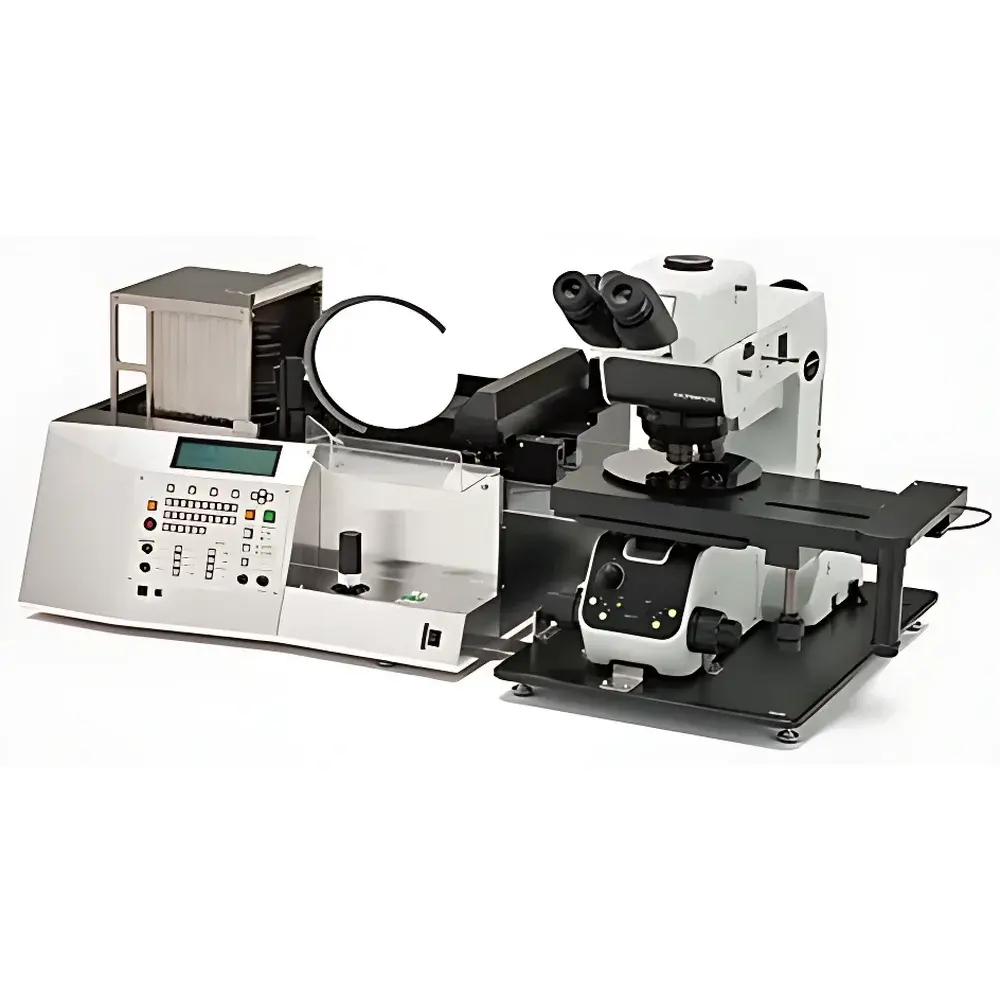
Olympus AL120 Semiconductor Wafer Handling and Inspection Microscope
| Brand | Olympus |
|---|---|
| Origin | Japan |
| Manufacturer Type | Manufacturer |
| Origin Category | Imported |
| Model | AL120 |
| Pricing | Upon Request |
Overview
The Olympus AL120 is a purpose-built, high-precision tool measuring microscope engineered specifically for semiconductor wafer handling and defect inspection in front-end and back-end fabrication environments. Designed around the core principles of non-contact optical alignment, vacuum-assisted stabilization, and modular configurability, the AL120 integrates advanced optical metrology with industrial-grade automation to support rigorous quality control workflows. Its optical architecture leverages the proven Olympus MX-series platform—renowned for its mechanical rigidity, thermal stability, and compatibility with multiple contrast modalities—including brightfield, darkfield, differential interference contrast (DIC), near-infrared (NIR), and deep ultraviolet (DUV) illumination. This multimodal capability enables reliable visualization of surface topography, edge defects, micro-scratches, particulate contamination, and lithographic pattern fidelity across silicon, SOI, compound semiconductor, and thin-film substrates.
Key Features
- Three configurable wafer size variants: dedicated 200 mm, dual-mode 200/150 mm, and 150 mm (supporting wafers ≤150 mm in diameter)
- Two inspection architecture options: L-type for high-magnification micro-inspection only, and LMB-type for combined macro/micro inspection with integrated handling
- Ultra-thin wafer handling capability: LMB-90 configuration supports automated transport of full cassettes (25 wafers) of 90 µm-thick substrates using a newly engineered low-force robotic arm
- 360° rotatable macro inspection arm for full-circumference visual assessment of wafer edges, backside, and bevel regions—enabling detection of micro-scratches, chipping, and particle adhesion without repositioning
- Motorized tilt function (up to ±30°) during surface macro inspection for optimized oblique-angle defect characterization
- Non-contact optical notch/flat identification system minimizing physical contact and preserving wafer cleanliness and surface integrity
- Front-loading cassette station compliant with SEMI S2/S8 safety standards and RoHS Directive 2011/65/EU environmental requirements
- Electric objective turret synchronized with motorized aperture diaphragm to maintain optimal Köhler illumination and contrast for each magnification level
Sample Compatibility & Compliance
The AL120 accommodates standard semiconductor wafer formats including 100 mm, 150 mm, and 200 mm diameters, with optional configurations supporting specialty substrates such as glass, sapphire, and GaAs. Thickness compatibility spans 50 µm to 1,000 µm, with specialized handling modules certified for ultra-thin wafers down to 75 µm (validated per JEDEC JESD22-A108F handling stress protocols). All mechanical and optical subsystems conform to ISO 10110-7 (optical element surface quality), ISO 9001:2015 (quality management), and SEMI E10 (definition and measurement of equipment reliability). The system’s vacuum chuck design meets SEMI F47-0201 voltage sag immunity requirements, ensuring stable operation during power fluctuations common in fab utilities infrastructure.
Software & Data Management
The AL120 operates via an embedded real-time control interface featuring a high-resolution LCD display with intuitive icon-based navigation. Up to 10 user-defined inspection programs can be stored—each specifying cassette type, wafer position mapping, stage velocity profiles, illumination mode, and focus parameters. A dedicated RECALL function retrieves previously flagged defective slots (SLOT IDs) directly from inspection logs, enabling rapid re-evaluation without manual navigation. While the base system does not include PC-hosted software, it provides RS-232 and Ethernet interfaces for integration into factory-wide MES or SPC platforms. Optional firmware upgrades support audit trail logging aligned with FDA 21 CFR Part 11 requirements—including electronic signatures, time-stamped event records, and immutable parameter change history—facilitating GLP/GMP-compliant documentation in regulated R&D and pilot-line environments.
Applications
- Pre-bond and post-bond wafer inspection for TSV, hybrid bonding, and direct wafer bonding processes
- Edge defect screening prior to epitaxial growth or CMP steps
- Backside contamination and micro-crack detection in thinned wafers
- Mask alignment verification and reticle defect triage in photomask shops
- Failure analysis sample positioning and preliminary defect localization in FA labs
- Process qualification for new substrate materials (e.g., SiC, GaN-on-Si) requiring high-contrast NIR/DIC imaging
FAQ
Does the AL120 support automated defect classification?
No—the AL120 is a manual and semi-automated inspection platform; defect classification requires integration with third-party machine vision software via digital video output.
Can the AL120 be retrofitted with motorized Z-focus?
Yes—Olympus offers optional motorized fine-focus modules compatible with all AL120 variants, enabling repeatable focus stacking and height profiling.
Is the vacuum chuck compatible with porous or low-dielectric-constant (low-k) wafers?
Yes—adjustable vacuum pressure settings (5–30 kPa range) and multi-zone suction control prevent deformation or cracking of fragile low-k dielectrics and MEMS devices.
What maintenance intervals are recommended for the robotic handling arm?
Olympus recommends preventive maintenance every 6 months or after 10,000 wafer-handling cycles, including arm calibration, vacuum seal inspection, and encoder verification per service bulletin AL120-SV-2023-04.
Does the AL120 meet cleanroom Class 100 (ISO 5) compatibility requirements?
The AL120 itself is not rated for ISO 5 operation; however, it is routinely installed in ISO 7/Class 10,000 cleanrooms with optional laminar flow hoods and static-dissipative housing kits available upon request.


