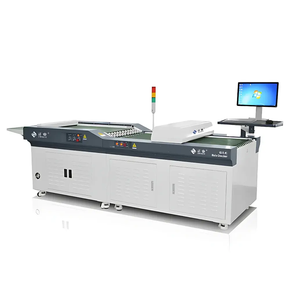
Online Hole Inspection System JK5200 by Zhengye
| Brand | Zhengye |
|---|---|
| Origin | Guangdong, China |
| Manufacturer Type | Manufacturer |
| Country of Origin | China |
| Model | JK5200 |
| Price Range | USD 14,000 – 70,000 |
| Repeatability | ±30 µm (standard round holes), ±75 µm (slot holes), ±150 µm (irregular holes) |
| Measurement Accuracy | ±20 µm (hole diameter ≤ 1 mm), ±30 µm (1 mm < diameter < 4 mm), ±40 µm (diameter ≥ 4 mm) |
| Inspection Speed | 3.0–8.0 m/min (drilled panels), 6.5–12.5 m/min (finished PCBs) |
| Detectable Hole Diameter | 0.1–10.0 mm |
| Max. Panel Size | 630 mm × 650 mm |
| Min. Panel Size | 80 mm × 100 mm |
| Panel Thickness | 0.3–10.0 mm |
| Minimum Edge-to-Hole Distance | ≥ 0.10 mm |
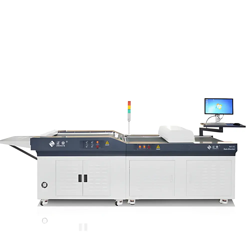
| Dimensions (L×W×H) | 3510 mm × 1160 mm × 1100 mm |
| Weight | ~800 kg |
Overview
The Zhengye JK5200 Online Hole Inspection System is an industrial-grade, vision-based in-line metrology platform engineered for automated, non-contact inspection of printed circuit board (PCB) holes immediately after drilling and prior to final packaging. It operates on high-resolution contact image sensor (CIS) scanning technology combined with deterministic sub-pixel edge detection algorithms and real-time geometric feature extraction. Unlike manual or offline coordinate measuring machines (CMMs), the JK5200 integrates directly into PCB production lines—enabling 100% inline screening without process interruption. Its core function is quantitative verification of hole count, positional accuracy, dimensional conformity (diameter, slot length/width), and surface-level defect classification—including plugging, foreign material intrusion, misdrilling, breakout, and edge proximity violations. The system delivers binary OK/NG output per panel, synchronized with factory automation protocols (e.g., SECS/GEM, Modbus TCP), ensuring traceability and statistical process control (SPC) readiness.
Key Features
- High-precision CIS imaging module with calibrated optical magnification and uniform LED illumination, optimized for copper-clad FR-4, polyimide, and metal-core substrates.
- Dual-lane parallel inspection architecture: supports simultaneous scanning of two PCBs at independent speeds—maximizing throughput without compromising measurement fidelity.
- Automated fiducial-based registration: compensates for panel warpage, thermal drift, and mechanical translation using multi-point reference alignment and affine transformation correction.
- Real-time defect annotation engine: overlays pixel-accurate bounding boxes and measurement tags directly onto inspection images, with configurable severity thresholds for each defect class.
- Networked repair station interface: enables remote access via standard web browsers; multiple engineering workstations can concurrently view NG panels, annotate root causes, and push corrective feedback to the line operator terminal.
- Ruggedized industrial enclosure (IP54-rated) with vibration-dampened base frame, designed for continuous operation in Class 10,000 cleanroom environments typical of high-mix PCB fabrication facilities.
Sample Compatibility & Compliance
The JK5200 accommodates rigid, flex, and rigid-flex PCBs across standard industry thicknesses (0.3–10.0 mm) and aspect ratios. It reliably inspects microvias (≥0.1 mm), through-holes, and complex slot geometries—even on panels with solder mask, silkscreen, or surface finish variations (ENIG, immersion silver, OSP). All measurement algorithms comply with IPC-A-600 and IPC-6012 requirements for hole quality assessment. Data audit trails meet GLP/GMP documentation standards, including timestamped operator logins, parameter change history, and calibration event records. Optional FDA 21 CFR Part 11-compliant software package available for regulated medical electronics manufacturing.
Software & Data Management
The embedded inspection software runs on a real-time Linux OS with deterministic I/O scheduling. It includes a modular GUI supporting multilingual UI (English, Simplified Chinese, Japanese), configurable pass/fail logic trees, and SPC dashboard integration (X-bar/R charts, Cp/Cpk calculation). Raw image archives, measurement CSV exports, and defect heatmaps are stored locally on RAID-1 SSD arrays or streamed to network-attached storage (NAS) via SMB/NFS. RESTful API enables bidirectional data exchange with MES (e.g., Siemens Opcenter, Rockwell FactoryTalk) and QMS platforms. Calibration certificates are digitally signed and exportable in PDF/A-1b format per ISO/IEC 17025 guidelines.
Applications
- Final verification of drill accuracy in HDI and high-layer-count PCBs prior to electroplating and lamination.
- Post-drill quality gate for automotive ADAS modules, where hole positional deviation directly impacts impedance-controlled via stitching.
- In-process monitoring for aerospace-grade polyimide flex circuits requiring zero tolerance for slot-length variation.
- Supplier qualification audits: generates standardized inspection reports accepted by Tier-1 OEMs under AS9100 Rev D clause 8.6.2.
- Root cause analysis support: correlates hole defects with upstream drill bit wear data, feed rate logs, and coolant pressure metrics.
FAQ
What types of defects does the JK5200 detect beyond missing or oversized holes?
It identifies plugging (resin/copper debris), foreign object contamination (fibers, solder balls), slot asymmetry, broken annular rings, and edge-distance violations—classified per IPC-6012 section 3.7.2.
Can the system be integrated with existing factory automation infrastructure?
Yes—it supports Ethernet/IP, Modbus TCP, and SECS/GEM communication protocols; PLC-triggered start/stop, hardware I/O handshaking, and digital twin synchronization are standard.
Is periodic recalibration required, and how is it performed?
Annual traceable calibration against NIST-traceable step gauges is recommended; on-site calibration routines include lens distortion mapping, illumination uniformity profiling, and edge detection repeatability validation—fully documented in the calibration management module.
Does the system support custom measurement definitions for proprietary hole patterns?
Yes—users define custom geometric templates (e.g., staggered arrays, elliptical apertures) via CAD import (Gerber RS-274X, ODB++) and apply rule-based tolerancing per feature group.
What maintenance intervals are specified for long-term reliability?
Scheduled preventive maintenance every 6 months includes CIS sensor cleaning, air filtration replacement, motion system lubrication, and thermal stability verification—log entries auto-sync to CMMS via CSV export.