
PELCO FlipScribe Backside Scribing Tool for Semiconductor Wafers
| Brand | Ted Pella |
|---|---|
| Origin | USA |
| Manufacturer Type | Authorized Distributor |
| Origin Category | Imported |
| Model | FlipScribe |
| Maximum Scribing Speed | Manual Operation |
| Application Scope | Semiconductor Wafer Dicing, Backside Alignment Scribing, Brittle Substrate Preparation |
Overview
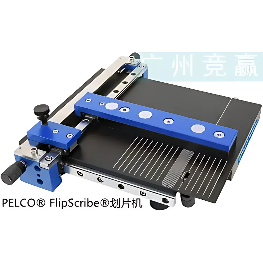
The PELCO® FlipScribe is a precision-engineered, purely mechanical backside scribing instrument designed for controlled, non-destructive groove formation on semiconductor wafers and brittle substrates prior to cleavage or dicing. Unlike conventional front-side scribers or motorized dicing saws, the FlipScribe operates on a fundamental principle of kinematic alignment: it positions a hardened diamond scribing tip *beneath* the sample—on its backside—while enabling real-time visual confirmation of scribe location on the device-facing surface through optical microscopy or direct observation. This configuration eliminates physical contact with patterned or metallized top surfaces, preserving critical microstructures, thin-film integrity, and contamination-sensitive features. The tool leverages rigid mechanical registration—via integrated guide fences, calibrated micrometer-adjustable scribe height and tilt, and an embedded metric scale—to deliver repeatable scribe placement with ±200 µm positional accuracy. Its design conforms to standard laboratory workflows in semiconductor process development, failure analysis (FA), and academic microfabrication, where low-cost, rapid prototyping of diced dies or test structures is required without cleanroom-grade infrastructure.
Key Features
- Purely mechanical operation—no electrical power, vacuum, or compressed air required; ideal for benchtop use in shared labs or gloveboxes.
- Backside-mounted diamond scribe (industrial-grade, fixed-point geometry) ensures zero top-surface contact during groove initiation and propagation.
- Adjustable scribe height and angular tilt enable optimization for varying substrate thicknesses (e.g., 100–650 µm Si wafers) and crystallographic orientation (e.g., , cleavage planes).
- Integrated linear guide fence and engraved metric scale (0.1 mm resolution) support rapid, reproducible alignment—typical setup and scribing completed within 60 seconds per line.
- Modular scribe stop (“scribing shield”) allows precise definition of scribe length from 1 mm to 100 mm, facilitating controlled size reduction of large-area substrates (e.g., 4″–6″ wafers, glass slides, sapphire blanks).
- Compatible with bonded wafer stacks (e.g., Si-SiO₂-Si), amorphous substrates (fused silica, quartz), and single-crystal materials (Si, GaAs, sapphire, LiNbO₃) without delamination risk.
Sample Compatibility & Compliance
The FlipScribe accommodates substrates up to 150 mm in diameter and 5 mm in thickness, including but not limited to silicon, silicon carbide (SiC), gallium nitride (GaN), indium phosphide (InP), fused quartz, borosilicate glass, and alumina ceramics. Its mechanical architecture complies with ISO 14644-1 Class 8 cleanroom handling requirements when used with appropriate gloves and lint-free wipes. While not certified to SEMI standards, the tool supports processes aligned with SEMI F20 (Wafer Handling) and SEMI F47 (Mechanical Integrity of Wafer Chucks) best practices. No software or electronic control system is present; therefore, no FDA 21 CFR Part 11 or IEC 62304 compliance claims apply—consistent with its role as a manual pre-dicing alignment aid rather than a production-grade dicing system.
Software & Data Management
None. The FlipScribe contains no embedded electronics, firmware, or digital interface. All operation is tactile and visually guided. No data logging, audit trail, or user authentication is implemented—making it inherently compliant with environments requiring minimal validation overhead (e.g., academic research labs, preliminary FA stages, or GLP-aligned material characterization where manual process records suffice). Users document scribe parameters (position, length, tilt angle) via lab notebook entries or LIMS-integrated SOP checklists.
Applications
- Precise backside scribing of bonded SOI or heterostructure wafers prior to thermal or mechanical cleavage.
- Preparation of test chips from full wafers without exposing active circuitry to mechanical stress or debris.
- Controlled fracturing of MEMS devices, photonic crystals, and piezoelectric substrates where front-side integrity is paramount.
- Rapid prototyping of diced samples for cross-sectional SEM/TEM specimen preparation (e.g., lift-out targets).
- Alignment reference marking on transparent or reflective substrates (e.g., sapphire LED wafers) using optical microscope-assisted positioning.
- Teaching tool in semiconductor fabrication courses for demonstrating crystallographic cleavage behavior and scribe-induced fracture mechanics.
FAQ
Is the FlipScribe compatible with automated wafer handling systems?
No—it is a manual, benchtop-only tool requiring operator intervention for loading, alignment, and scribing.
Can it be used on 8-inch or larger wafers?
No—maximum supported substrate diameter is 150 mm (6 inches); larger wafers exceed platform clearance and guide fence reach.
Does the diamond scribe require periodic replacement or recalibration?
Yes—the scribe tip is consumable and should be inspected under ≥100× magnification before each use; replacement kits (part #FLIP-SCRIBE-TIP) are available from Ted Pella.
What is the minimum scribe line width achievable?
Line width depends on applied force and substrate hardness; typical grooves range from 5–15 µm wide under standard hand-pressure operation.
Is training or certification required to operate the FlipScribe?
No formal certification is required, but users should complete internal SOP familiarization covering scribe tip handling, alignment verification, and cleavage technique to ensure consistent results.


