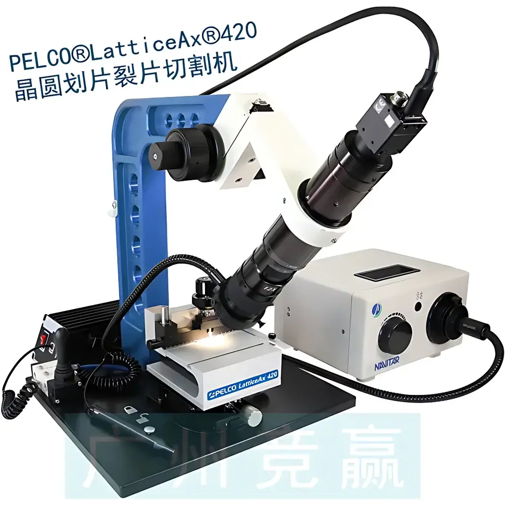
PELCO® LatticeAx® 420 Wafer Cleaving and Scribing System
| Brand | Ted Pella |
|---|---|
| Origin | USA |
| Manufacturer Type | Authorized Distributor |
| Origin Category | Imported |
| Model | LatticeAx 420 |
| Maximum Linear Scribing Speed | 600 µm/s |
| Application Scope | Semiconductor Wafers, MEMS, Compound Semiconductors (SiC, GaN), Optical Substrates, and Research-Scale Device Fabrication |
Overview
The PELCO® LatticeAx® 420 is a precision-engineered wafer cleaving and scribing system designed for controlled, non-destructive separation of brittle crystalline materials—primarily semiconductor wafers, MEMS substrates, and optoelectronic crystals. Unlike conventional dicing saws that rely on abrasive blade cutting or laser ablation, the LatticeAx 420 employs mechanical lattice cleavage: a diamond-tipped indenter creates a sub-millimeter, nanoscale-controlled stress initiation line (typically <1 mm in length and ~10 µm wide) on the wafer surface, followed by controlled fracture propagation along crystallographic planes. This method leverages intrinsic material anisotropy to achieve atomically aligned, low-damage separation with minimal kerf loss, zero thermal influence, and no debris generation—critical for preserving device integrity in R&D, prototyping, and small-batch fabrication environments.
Key Features
- High-resolution optical navigation: Integrated monocular confocal zoom lens (0.58–7× magnification) with 4 µm optical resolution and motorized coarse/fine focus control for precise feature identification and alignment.
- Digital imaging suite: Full-color CCD camera with real-time image capture, on-screen crosshair overlay, and live contrast-enhanced display—enabling rapid verification of crystal orientation and cleave line placement.
- Micrometer-precision motion control: X-Y translation stage with manual ergonomic knobs offering 5 µm incremental positioning resolution and ±10 µm absolute target repeatability.
- Crystallography-aware cleaving: Diamond indenter tip (standard 100 µm radius, optional custom geometries) delivers consistent, shallow indentation depth (sub-100 nm) optimized for {100}, {110}, and {111} silicon orientations—as well as SiC, GaAs, and sapphire substrates.
- Compact benchtop architecture: Footprint under 400 × 350 mm; operates without vacuum, compressed air, or external cooling—suitable for cleanroom Class 1000+ and general lab environments.
- Ergonomic design: Adjustable height base, intuitive tactile controls, and integrated LED illumination minimize operator fatigue during extended use sessions.
Sample Compatibility & Compliance
The LatticeAx 420 accommodates wafers from 50 mm to 200 mm diameter (with optional chucks), including silicon, gallium arsenide, silicon carbide, lithium niobate, fused silica, and other single-crystal substrates exhibiting defined cleavage planes. It supports both front-side and back-side alignment workflows. The system complies with ISO 14644-1 (cleanroom particulate standards) and meets mechanical safety requirements per ANSI B11.19. While not a GMP production tool, its deterministic, user-independent process enables traceable, auditable cleaving protocols suitable for GLP-compliant research laboratories and pre-fab characterization workflows. All mechanical adjustments are lockable and documented via operator log entries in associated software.
Software & Data Management
The LatticeAx 420 operates via a dedicated Windows-based control interface supporting image annotation, coordinate logging, and session history export (CSV/Excel). Each cleave event records timestamp, stage coordinates, magnification level, and operator ID—providing full audit trail capability. Software adheres to FDA 21 CFR Part 11 principles for electronic records: digital signatures, user authentication, and immutable event logs are available upon configuration with enterprise IT infrastructure. No cloud connectivity or remote telemetry is embedded; data remains local unless explicitly exported.
Applications
- Pre-dicing metrology sample preparation for TEM, SEM, and cross-sectional FIB-SEM analysis.
- Rapid prototyping of photonic integrated circuits (PICs) and micro-optoelectromechanical systems (MOEMS).
- Cleaving of fragile heterostructures (e.g., 2D material stacks, perovskite thin films) where thermal or mechanical shock must be avoided.
- Failure analysis (FA) labs requiring undamaged die isolation prior to decapsulation or electrical probing.
- Academic and government research facilities performing crystal growth validation, dislocation mapping, and epitaxial layer quality assessment.
- Calibration reference specimen preparation for AFM tip wear studies and nanoindentation standardization.
FAQ
Does the LatticeAx 420 require consumables beyond the diamond indenter tip?
No—only periodic replacement of the indenter tip (typical lifetime >5,000 cleaves on Si wafers) and standard optical cleaning supplies are needed.
Can it process wafers with patterned topography or metal layers?
Yes—the system accommodates up to 20 µm total topography variation; thin-film metallization does not impede cleavage if underlying substrate retains crystallinity.
Is training required for operational qualification?
Basic operation can be mastered in under 5 minutes; advanced techniques (e.g., off-axis cleaving, multi-step fracture initiation) are covered in the included 2-hour video curriculum and PDF protocol library.
What maintenance intervals are recommended?
Biannual optical calibration and annual stage lubrication—both documented in the onboard maintenance scheduler and accessible via the software interface.
Is the system compatible with automated wafer handling or integration into fab MES?
Not natively—but RS-232 and USB HID interfaces support third-party script-driven control for semi-automated batch processing in pilot-line settings.
Related Products


