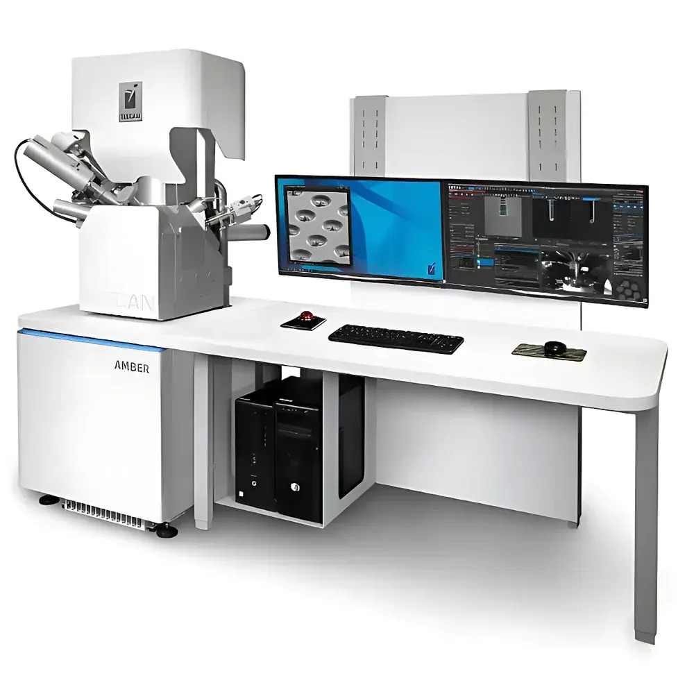
TESCAN AMBER Dual-Beam Focused Ion Beam Scanning Electron Microscope (FIB-SEM)
| Brand | TESCAN |
|---|---|
| Origin | Czech Republic |
| Model | TESCAN AMBER |
| Beam Sources | Schottky Field-Emission Electron Gun + Liquid-Metal Gallium Ion Source |
| SEM Resolution | ≤0.6 nm @ 30 kV (in-lens detection) |
| FIB Resolution | <2.5 nm @ 30 kV |
| Minimum FIB Acceleration Voltage | 500 V |
| Maximum FIB Current | 100 nA |
| Real-time Multi-channel Acquisition | Up to 8 Simultaneous Signals |
Overview
The TESCAN AMBER Dual-Beam FIB-SEM is an integrated analytical platform combining a high-performance field-emission scanning electron microscope (FE-SEM) and a gallium liquid-metal ion source focused ion beam (Ga-FIB) column within a single, co-axially aligned vacuum chamber. Engineered for precision nanoscale characterization and manipulation, the system operates on two complementary physical principles: electron–sample interactions (secondary electron, backscattered electron, X-ray emission) for non-destructive imaging and microanalysis; and ion–sample sputtering, deposition, and milling for site-specific sample preparation, cross-sectioning, and nanofabrication. Its dual-beam architecture enables real-time correlation between structural observation and targeted material modification—critical for TEM lamella preparation, atom probe tomography (APT) specimen lift-out, failure analysis in semiconductor devices, and 3D nanotomography. The AMBER platform is designed for rigorous laboratory environments requiring reproducible, traceable, and compliant workflows in both industrial R&D and academic research.
Key Features
- BrightBeam™ SEM Column: Features an electromagnetic–electrostatic compound objective lens with a 70° polepiece geometry, delivering true magnetic-field-free ultra-high-resolution (UHR) imaging—essential for imaging magnetic materials without beam deflection or domain distortion.
- In-lens Axial Detector & Multi-Angle Signal Collection: Integrated in-beam axial SE/BSE detector combined with multi-segment solid-state detectors enables simultaneous acquisition of topographic, compositional, and crystallographic contrast at variable landing energies (0.1–30 keV).
- Schottky Field-Emission Electron Source: Delivers stable beam currents up to 400 nA with rapid energy switching (<10 ms), supporting high-current analytical modes (EDS, EBSD) and low-voltage surface-sensitive imaging.
- Orage™ Ga-FIB Column: Optimized for nanoscale milling fidelity and deposition control, achieving <2.5 nm resolution at 30 kV and operational stability down to 500 V acceleration voltage—enabling damage-free thinning of beam-sensitive materials.
- OptiGIS Gas Injection System: Modular, leak-tight gas delivery architecture supporting up to six independently controlled injectors for precise localized etching (e.g., XeF₂), deposition (e.g., Pt, W, C), and enhanced ion milling (e.g., H₂O, I₂).
- EquiPower™ Thermal Management: Active cooling and symmetric thermal design minimize thermal drift during long-duration acquisitions or sequential FIB/SEM operations, ensuring sub-nanometer positional repeatability over hours.
Sample Compatibility & Compliance
The TESCAN AMBER accommodates standard 150 mm SEM stubs and custom TEM grids, with stage travel of 100 × 100 × 40 mm (X/Y/Z) and tilt range of −10° to +90°. It supports conductive, semi-conductive, and insulating samples—enabled by low-voltage imaging (≤1 keV), beam deceleration technology (BDT), and optional charge compensation modules. All hardware and software components comply with CE marking requirements under the EU Machinery Directive 2006/42/EC and Electromagnetic Compatibility Directive 2014/30/EU. The system architecture supports audit-trail-enabled operation per FDA 21 CFR Part 11 when configured with TESCAN’s optional GLP/GMP-compliant software package, including electronic signatures, user access tiers, and immutable acquisition logs.
Software & Data Management
TESCAN’s Unified Workflows™ software provides an intuitive, task-oriented interface built on a modular, Python-scriptable framework. It unifies SEM imaging, FIB milling, automated serial sectioning (for 3D reconstruction), and correlative analysis (e.g., EDS mapping synchronized with FIB depth profiling) within a single environment. Data is stored in open-format HDF5 containers, ensuring long-term readability and compatibility with third-party analysis tools (e.g., Avizo, Dragonfly, HyperSpy). Real-time multi-channel acquisition supports up to eight synchronized signals—including SE, BSE, EDS, and ion-induced secondary electrons—each timestamped and georeferenced to stage coordinates. Raw data and processing parameters are automatically embedded in metadata, fulfilling FAIR (Findable, Accessible, Interoperable, Reusable) principles for scientific data stewardship.
Applications
- Preparation of electron-transparent lamellae for transmission electron microscopy (TEM) and scanning transmission electron microscopy (STEM), including site-specific lift-out from IC devices and battery cathode particles.
- Atom probe tomography (APT) specimen fabrication with sub-50 nm tip radius control and minimal surface amorphization.
- 3D nanotomography via automated serial sectioning and slice-and-view reconstruction, applied to porous media, composite interfaces, and biological mineralized tissues.
- Failure analysis of advanced packaging structures (e.g., TSVs, microbumps) through cross-sectional imaging and elemental depth profiling.
- Nanoscale prototyping: direct-write deposition of metallic interconnects, insulating barriers, or catalytic nanostructures using ion-induced chemistry.
- In-situ electrical testing: integration with nanoprobers and biasing stages for correlated structural–electrical characterization of memristors and 2D material devices.
FAQ
What is the minimum accelerating voltage for the Ga-FIB column?
The Orage™ Ga-FIB column operates down to 500 V, enabling ultra-low-energy milling with minimized subsurface damage.
Can the system image magnetic samples without artifacts?
Yes—the BrightBeam™ column produces a magnetically neutral imaging environment, eliminating Lorentz deflection and preserving domain contrast in ferromagnetic and antiferromagnetic materials.
How many gas injection systems can be installed simultaneously?
Up to six independent OptiGIS units can be mounted, supporting multi-chemistry workflows such as sequential etching/deposition cycles.
Is the software compatible with automated 3D reconstruction pipelines?
Yes—Unified Workflows™ includes native support for serial block-face imaging, fiducial-based alignment, and export to standard 3D visualization formats (e.g., TIFF stacks, NRRD, STL).
Does the system meet regulatory requirements for GxP laboratories?
When equipped with the optional Compliance Edition software, the AMBER supports 21 CFR Part 11 compliance, including role-based access control, electronic signatures, and full audit trail generation.


