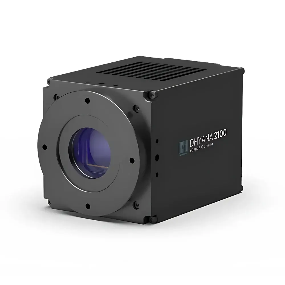
Tucsen Dhyana 2100 Scientific CMOS Camera
| Brand | Tucsen |
|---|---|
| Origin | Fujian, China |
| Manufacturer Type | OEM Manufacturer |
| Region of Origin | Domestic (China) |
| Model | Dhyana 2100 |
| Image Resolution | 5120 (H) × 4096 (V) |
| Pixel Size | 4.5 µm × 4.5 µm |
| Sensor Active Area | 23.04 mm (H) × 18.43 mm (V) |
| Readout Speed | 975 fps @ 12-bit (Fast Binning Mode) |
| Quantum Efficiency | 63% @ 520 nm |
| Sensor Type | Front-Side Illuminated (FSI) CMOS |
| Full-Well Capacity | 32 ke⁻ (12-bit, Gain 0), 120 ke⁻ (Binned) |
| Dynamic Range | 68.8 dB (12-bit, Gain 2) |
| Read Noise | 3.5 e⁻ (typ., 12-bit) |
| Shutter Type | Global |
| Exposure Time | 4 µs – 10 s |
| Dark Signal Non-Uniformity | 1.1 e⁻ |
| Photoresponse Non-Uniformity | 0.15% (12-bit, Gain 0), 0.45% (12-bit, Gain 3) |
| Cooling Method | Air + Liquid |
| Max ΔT | 25 °C (Air), 30 °C (Liquid) |
| Binning Modes | 2×2, 4×4, 8×8 |
| ROI Support | Yes |
| Trigger Interface | Hirose |
| Data Interface | CXP-12 ×8 (Full Mode), CXP-12 ×4 (Base Mode) |
| Bit Depth | 8/10/12-bit |
| Optical Mount | M58 / F-Mount / Customizable |
| Power | 24 V / 6.67 A |
| Max Power Consumption | ≤120 W |
| Dimensions | 95 mm × 95 mm × 140 mm (excl. water fittings) |
| Weight | <1850 g |
| Operating Temperature | 0–40 °C |
| Humidity | 10–85% RH |
Overview
The Tucsen Dhyana 2100 is a high-performance scientific CMOS (sCMOS) camera engineered for demanding optical imaging applications requiring simultaneous high spatial resolution, temporal fidelity, and photon-limited sensitivity. Built around the Gpixel GSPRINT4521 front-side illuminated (FSI) sensor, it delivers 21.1 megapixels (5120 × 4096) with a 4.5 µm pixel pitch and a 29.5 mm diagonal optical format—enabling wide-field coverage without sacrificing detail. Its global shutter architecture eliminates motion distortion in fast dynamic processes, making it suitable for time-resolved semiconductor inspection, real-time wafer defect mapping, high-speed flat-panel display (FPD) characterization, voltage-sensitive fluorescence imaging, and cardiac motion analysis in preclinical models. The camera’s dual-stage thermal management—combining active air and liquid cooling—stabilizes sensor temperature to suppress dark current drift and ensure measurement repeatability across extended acquisition sessions, a critical requirement for quantitative intensity calibration in GLP-compliant labs.
Key Features
- Ultra-High Frame Rates: Up to 975 fps at 12-bit depth in Fast Binning mode (8×8), enabling high-throughput capture of transient phenomena while preserving signal-to-noise ratio through effective pixel aggregation.
- Global Shutter Precision: Eliminates rolling-shutter artifacts during rapid stage motion or pulsed illumination—essential for synchronized metrology in semiconductor lithography verification and mask inspection.
- Deep-Cooling Architecture: Achieves up to 30 °C ΔT below coolant temperature via integrated liquid cooling; reduces dark current to sub-0.01 e⁻/pix/s at −10 °C sensor temperature, supporting long-exposure low-light applications such as voltage-sensitive dye imaging in electrophysiology.
- Low-Noise Readout: Typical read noise of 3.5 e⁻ at 12-bit gain settings ensures high-fidelity quantification in photon-starved conditions, validated per EMVA 1288 standards.
- Flexible Data Throughput: CXP-12 interface (CoaXPress v2.0) supports scalable bandwidth: 8-lane configuration (up to 12 Gbps) for full-resolution streaming; 4-lane for base-mode operation—compatible with industry-standard frame grabbers and real-time processing platforms.
- Configurable Imaging Modes: Hardware-supported region-of-interest (ROI), binning (2×2 to 8×8), and multi-gain readout paths allow optimization for specific SNR, speed, or dynamic range requirements—aligned with ASTM E3081-17 guidelines for digital imaging system characterization.
Sample Compatibility & Compliance
The Dhyana 2100 is compatible with standard optical interfaces including M58 and F-mount, and supports custom mechanical and optical integration for OEM systems deployed in cleanroom environments (ISO Class 5–7). Its monochrome sensor design maximizes quantum efficiency—63% peak at 520 nm—and avoids color interpolation artifacts, ensuring traceable intensity linearity required for ASTM E2594-17 (quantitative fluorescence microscopy) and ISO 15739:2013 (noise and dynamic range measurement). The camera firmware implements hardware-level trigger synchronization (exposure start/readout end signals via Hirose connector), supporting deterministic timing for multi-modal acquisition workflows compliant with FDA 21 CFR Part 11 electronic record integrity requirements when paired with validated acquisition software.
Software & Data Management
Tucsen provides the SamplePro SDK—a cross-platform (Windows/Linux), C/C++-based development toolkit—with full support for GenICam-compliant parameter control, real-time image buffering, and metadata embedding (including exposure time, gain, temperature, and binning mode). The SDK enables integration into automated test platforms used in semiconductor process control (e.g., inline wafer inspection stations) and biomedical research systems subject to ISO/IEC 17025 accreditation. All acquired frames include embedded timestamping (µs resolution) and sensor thermal telemetry, facilitating post-acquisition drift correction and audit-trail generation for GLP/GMP documentation. Raw 12-bit data is stored in lossless TIFF or HDF5 formats, preserving bit-depth fidelity for downstream spectral unmixing or deconvolution pipelines.
Applications
- Semiconductor & Wafer Inspection: High-speed detection of micro-defects, pattern fidelity assessment, and overlay error metrology under UV or visible illumination.
- Flat-Panel Display (FPD) Testing: Real-time uniformity evaluation, mura defect identification, and response-time characterization at production-line speeds.
- Voltage-Sensitive Imaging: Sub-millisecond tracking of membrane potential changes in neuronal or cardiac tissue using fast-response fluorescent dyes (e.g., ArcLight, ASAP).
- High-Speed Aerial Imaging: Onboard payload for UAV-based multispectral surveying where compact form factor, low power draw (<120 W), and robust thermal design are critical.
- Preclinical Cardiac Imaging: Synchronized cine acquisition of Langendorff-perfused heart preparations with motion artifact suppression via global shutter and precise external triggering.
FAQ
Does the Dhyana 2100 support hardware-triggered acquisition with sub-microsecond jitter?
Yes—the Hirose-trigger interface provides TTL-compatible input/output signals with hardware-level synchronization and jitter < 100 ns, enabling deterministic frame alignment with laser pulses or stage encoders.
Is the camera compatible with third-party acquisition software such as Micro-Manager or NIS-Elements?
Yes—via GenICam-compliant drivers and standardized XML feature descriptions, ensuring interoperability with major microscopy and industrial imaging platforms.
What is the maximum sustained acquisition duration at full resolution and 450 fps?
With active liquid cooling (coolant inlet ≤20 °C), continuous acquisition exceeds 2 hours without thermal-induced gain drift or dark current increase beyond ±1.5% of baseline.
Can the Dhyana 2100 be integrated into a vacuum or nitrogen-purged optical enclosure?
Yes—custom variants with sealed housings and feedthrough-compatible connectors are available upon request for controlled-atmosphere applications.
How is calibration data (e.g., PRNU, DSNU) delivered and maintained?
Factory-measured non-uniformity maps are provided in IEEE 1609-compliant format and can be applied in real time via SDK; users may also perform field recalibration using uniform illumination sources per ISO 15739 Annex B protocols.


