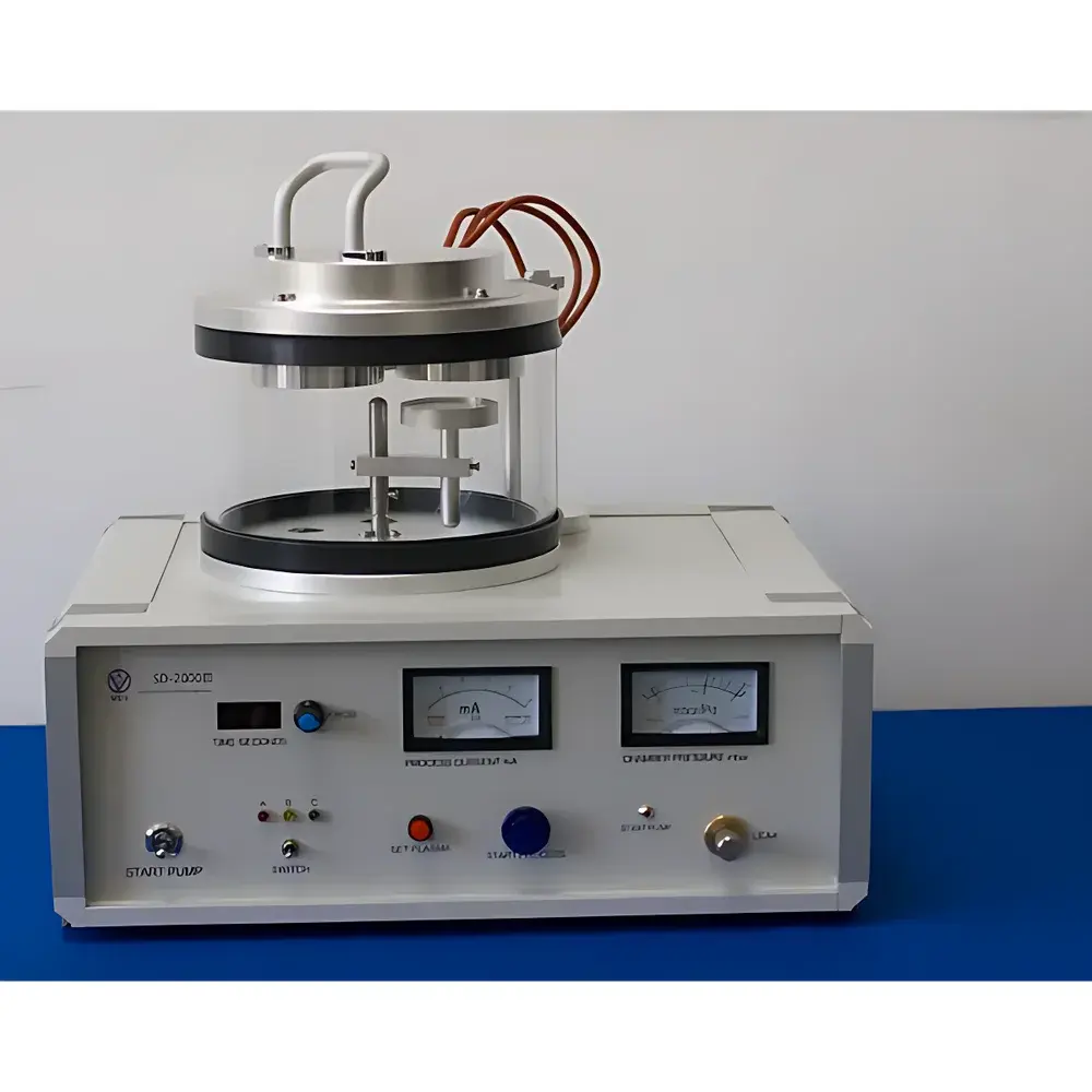
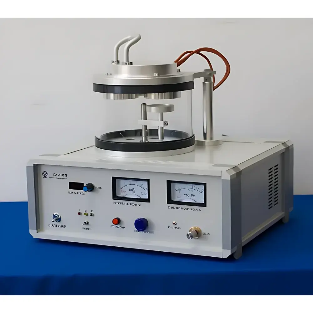
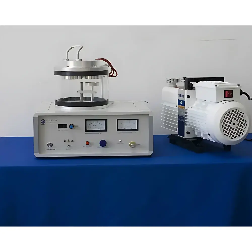

VPI SD-2000Ⅲ Triple-Target Magnetron Sputter Coater
| Brand | VPI (BoYuan Micro-Nano) |
|---|---|
| Origin | Beijing, China |
| Model | SD-2000Ⅲ |
| Target Materials | Au, Pt, Ag (Ø50 mm) |
| Control Mode | Automatic sample stage rotation synchronized with selected target |
| Chamber Dimensions | Ø160 mm × 120 mm (H) |
| Sample Stage | Ø50–70 mm, vertically adjustable |
| Sputtering Gases | Ar, N₂, and other process gases |
Overview
The VPI SD-2000Ⅲ Triple-Target Magnetron Sputter Coater is a compact, benchtop thin-film deposition system engineered for precision surface modification and conductive coating of non-conductive specimens in electron microscopy (EM), materials science, and nanotechnology laboratories. It operates on the principle of DC magnetron sputtering—where energetic argon ions, accelerated by a high-voltage negative bias (up to –1600 VDC), bombard solid metallic targets (Au, Pt, or Ag), ejecting atoms that condense uniformly onto substrates placed on a rotating, height-adjustable sample stage. This physical vapor deposition (PVD) technique ensures nanoscale control over film thickness, morphology, and composition without thermal damage to heat-sensitive samples—a critical requirement for biological specimens, polymers, and delicate nanostructures.
Key Features
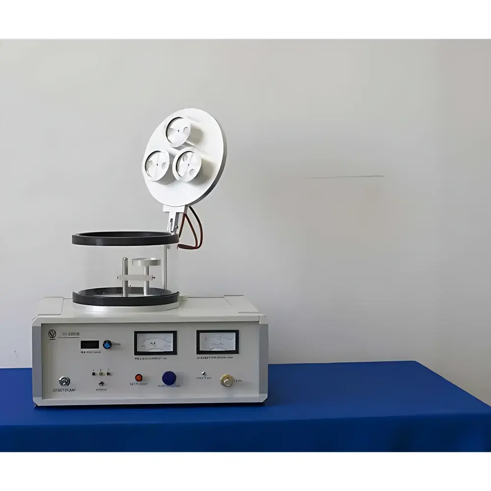
- Triple independent magnetron targets: Pre-installed 50 mm diameter Au, Pt, and Ag targets enable rapid, tool-free switching between conductive coatings—eliminating cross-contamination and reducing setup time between experiments.
- Automated rotational sample stage: The stage rotates synchronously with the selected target to ensure uniform angular coverage and consistent film thickness across the entire specimen area (Ø50–70 mm), meeting ASTM E2489–22 requirements for EM sample preparation reproducibility.
- Optically transparent chamber: Constructed from borosilicate glass (Ø170 mm × 130 mm), the chamber allows real-time visual monitoring of plasma ignition, target erosion, and sputter uniformity—supporting operator training and process troubleshooting.
- Stable vacuum architecture: Integrated 2 L/s mechanical pump achieves base pressure ≤4×10⁻² mbar; gas inlet port (Ø3 mm) supports precise flow control of Ar, N₂, or reactive mixtures for alloy or compound film synthesis.
- Digital process control: 0–999 s programmable timer with ±1 s resolution and continuously adjustable sputter rate (0–40 nm/min) enable repeatable deposition protocols compliant with GLP documentation standards.
Sample Compatibility & Compliance
The SD-2000Ⅲ accommodates standard EM stubs (Ø25 mm, Ø32 mm), silicon wafers (up to Ø50 mm), TEM grids, and irregularly shaped substrates up to 70 mm in diameter. Its low-energy, room-temperature sputtering process preserves structural integrity of beam-sensitive organic, polymeric, and biological samples—including freeze-dried tissues, pollen grains, and polymer nanocomposites. The system meets ISO 14644-1 Class 8 cleanroom compatibility when operated in controlled environments and supports traceable calibration via external quartz crystal microbalance (QCM) integration (optional). All electrical components conform to IEC 61010-1 safety standards for laboratory equipment.
Software & Data Management
While the SD-2000Ⅲ operates via intuitive front-panel digital controls, its analog signal outputs (voltage, current, timer status) are compatible with third-party data acquisition systems for automated logging. For regulated environments (e.g., ISO/IEC 17025-accredited labs), optional RS-232 or USB interfaces support integration with LIMS platforms and enable audit-trail generation per FDA 21 CFR Part 11 requirements when paired with validated software. Process parameters—including sputter time, gas type, voltage, and current—are manually recorded in lab notebooks using standardized SOP templates provided in the user manual.
Applications
- Scanning Electron Microscopy (SEM) sample preparation: Ultra-thin (<5 nm), low-resistivity Au or Pt coatings minimize charging artifacts while preserving topographic fidelity of insulating specimens.
- Nanomaterial functionalization: Sequential or co-sputtered bimetallic films (e.g., Pt–Ag) for catalytic electrode development and surface-enhanced Raman spectroscopy (SERS) substrates.
- Thin-film sensor research: Deposition of tunable resistive layers for gas-sensing oxides or plasmonic biosensor interfaces.
- Academic teaching labs: Demonstrating PVD fundamentals, plasma physics, and thin-film characterization techniques aligned with undergraduate materials engineering curricula (e.g., ASM International’s “Materials Characterization” syllabus).
- Optical prototype fabrication: Preliminary metal layer deposition for interference filter stacks and anti-reflection coating studies.
FAQ
What vacuum level is required for stable plasma ignition?
A base pressure ≤4×10⁻² mbar is sufficient for reliable DC plasma initiation with Ar gas at 10–30 sccm flow rates.
Can the system deposit non-metallic films such as TiO₂ or SiO₂?
Yes—when equipped with RF power supply (optional upgrade) and ceramic or oxide targets, the chamber supports reactive sputtering in Ar/O₂ mixtures.
Is remote operation or automation supported?
The unit does not include built-in PC control; however, analog I/O ports allow integration with PLCs or LabVIEW-based automation for high-throughput workflows.
How often must the targets be replaced?
Under typical SEM coating use (10–20 s per session), Au and Pt targets last ≥500 hours; Ag targets require more frequent replacement due to oxidation sensitivity.
Does the system comply with electromagnetic compatibility (EMC) directives?
Yes—the enclosure and internal shielding meet EN 61326-1:2013 for electromagnetic emissions and immunity in laboratory settings.


