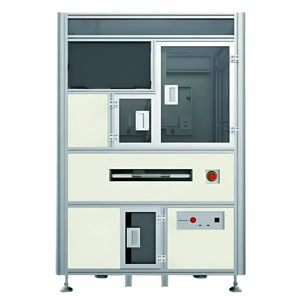
YCT WM5100 Automatic Wire Bond Metrology System
| Brand | YCT |
|---|---|
| Origin | Taiwan |
| Model | WM5100 |
| Application | Semiconductor Wire Bonding Process Inspection |
| Sample Handling | Vacuum Chuck Platform |
| Software | QX3000 Metrology Suite |
| Compliance | Supports SECS/GEM Interface |
| User Interface | Bilingual (English & Chinese) |
| Measurement Automation | CAD-based Program Import, Auto-Focus, Pass/Fail Thresholding, Audit-Trail Enabled Reporting |
Overview
The YCT WM5100 Automatic Wire Bond Metrology System is a precision optical metrology platform engineered for in-line and offline inspection of wire bonding processes in semiconductor packaging. It operates on high-resolution digital imaging combined with automated stage positioning and real-time focus control to quantify critical geometric parameters defined by JEDEC, IPC-7351, and industry-standard package qualification protocols. Unlike manual optical inspection or generic coordinate measuring machines, the WM5100 is purpose-built for bond geometry — capturing sub-micron dimensional features including ball shear height, ball diameter (Al/SnAg/Cu), first-bond (B1) and second-bond (B2) positional offsets, loop profile height, tail angle relative to die surface, and post-die-attach angular deviation. Its vacuum chuck ensures repeatable Z-axis referencing across wafers and leadframes, minimizing mechanical drift and enabling high reproducibility (<±0.5 µm repeatability under controlled lab conditions).
Key Features
- Vacuum-assisted sample stage with flatness tolerance ≤±1.2 µm over 150 mm × 150 mm area — guarantees consistent focal plane alignment across heterogeneous substrates (e.g., copper leadframes, ceramic packages, molded epoxy substrates).
- QX3000 metrology software with dual-language UI (English/Chinese), role-based access control (operator, engineer, admin), and configurable pass/fail tolerances per feature group.
- CAD-based programming workflow: import Gerber, ODB++, or DXF files to auto-generate measurement routines; supports layer mapping for bond pad coordinates and fiducial alignment.
- Intelligent auto-focus algorithm using contrast-based z-scan — achieves stable focus within ±0.3 µm vertical accuracy across varying reflectivity surfaces (e.g., Au-plated pads vs. black mold compound).
- SECS/GEM-compliant communication interface for integration into factory automation systems; supports HSMS over TCP/IP and message logging compliant with SEMI E30/E37 standards.
- Measurement traceability: all results include timestamp, operator ID, calibration status flag, and image thumbnail; audit trail records parameter edits, report exports, and user logins.
Sample Compatibility & Compliance
The WM5100 accommodates standard semiconductor packaging formats including QFP, SOP, SOIC, QFN, BGA, and WLCSP substrates up to 200 mm × 200 mm. It accepts both bare dies and fully assembled modules, provided bond wires are accessible from above (i.e., non-underfill or low-viscosity encapsulant scenarios). The system meets ISO 9001:2015 requirements for measurement process control and supports GLP/GMP documentation workflows via configurable reporting templates. All dimensional outputs comply with ASTM E29 rounding conventions and reference JESD22-B116 (wire bond pull test correlation) and IPC-A-610 Class 3 acceptance criteria for visual inspection.
Software & Data Management
QX3000 provides full metrology lifecycle management: from recipe creation and validation to statistical process monitoring (SPC). Each measurement sequence stores raw images, XY-stage coordinates, focus Z-value, and calibrated pixel-to-micron conversion coefficients. Reports export in PDF, CSV, and XML formats — with NG results highlighted in red and annotated with deviation magnitude and direction. Data can be archived locally or transmitted via SECS to MES or SPC servers. Optional FDA 21 CFR Part 11 compliance module enables electronic signatures, change history logging, and locked report generation for regulated environments.
Applications
- First-article inspection of new bond tooling setups (capillary, wedge, or ultrasonic transducer configurations).
- In-process verification during high-volume production ramp-up to validate bond parameter stability (e.g., loop height consistency across 10,000+ bonds).
- FMEA-driven root cause analysis for delamination, cratering, or non-stick failures — correlating geometry deviations with pull/shear test outcomes.
- Qualification of alternative wire materials (e.g., Cu vs. Au) where loop sag, ball deformation, and intermetallic growth impact reliability.
- Supporting AEC-Q200 stress testing by tracking dimensional drift pre/post temperature cycling or humidity exposure.
FAQ
Does the WM5100 support measurement of copper wire bonds?
Yes — the QX3000 software includes optimized illumination presets and edge-detection algorithms calibrated for copper’s lower reflectivity and higher oxidation sensitivity compared to gold.
Can measurement recipes be shared across multiple WM5100 units in a fab?
Yes — recipes are stored as portable .qxr files with embedded calibration metadata; version-controlled deployment is supported via network share or USB.
Is NIST-traceable calibration available for the WM5100?
YCT provides optional annual calibration services using certified step-height standards (NIST SRM 2160) and line-pitch gratings (NIST SRM 2058), documented per ISO/IEC 17025.
What is the minimum measurable ball diameter?
With 5 MP camera and 10× objective, the system resolves features down to 8 µm with measurement uncertainty <±0.4 µm (k=2) at 23 °C ±1 °C ambient.
How does the system handle warped or翘曲 substrates?
The vacuum chuck applies uniform pressure (≤–60 kPa) across the entire surface; for substrates exceeding 15 µm total indicator reading (TIR), optional Z-axis tilt compensation can be enabled during focus mapping.


