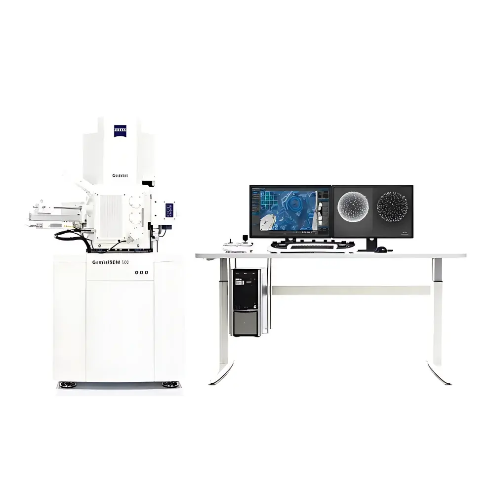
ZEISS GeminiSEM 500 Field Emission Scanning Electron Microscope
| Brand | ZEISS |
|---|---|
| Origin | Germany |
| Instrument Type | Floor-standing SEM |
| Electron Gun | Cold Field Emission (CFEG) |
| Secondary Electron Resolution | 0.5 nm @ 15 kV, 0.8 nm @ 1 kV (with Tandem Decel) |
| Magnification Range | 50× – 2,000,000× |
| Accelerating Voltage | 0.02 – 30 kV |
| Backscattered Electron Resolution | 1.0 nm @ 1 kV (ESB detector) |
| Detector Configuration | In-lens SE, ET-SE, optional ESB, aSTEM-4, EDS, EBSD, CL |
Overview
The ZEISS GeminiSEM 500 is a high-performance field emission scanning electron microscope engineered for nanoscale imaging and microanalysis across diverse scientific and industrial domains. Built upon the proprietary Gemini electron optical column—comprising a cold field emission gun (CFEG), Nano-twin lens objective, and integrated signal detection architecture—the system delivers exceptional surface sensitivity, high contrast, and sub-nanometer resolution at both high and low landing energies. Its core design principle centers on optimizing signal generation and collection efficiency under low-voltage conditions (≤1 kV), where conventional SEMs suffer from reduced signal-to-noise ratio, charging artifacts, and diminished surface detail fidelity. The GeminiSEM 500 achieves this through a combination of electrostatic-magnetic hybrid lensing, in-column energy filtering, and advanced deceleration physics—including the optional Tandem Decel stage biasing technology—which enables stable 0.8 nm secondary electron resolution at 1 kV without compromising beam coherence or detector efficiency. This makes it particularly suited for beam-sensitive polymers, biological specimens, uncoated ceramics, thin-film devices, and insulating materials requiring charge-free, high-fidelity topographic characterization.
Key Features
- Gemini II electron optical column with cold field emission source, delivering long-term beam stability (<0.2% intensity drift per hour) and minimal energy spread (ΔE < 0.3 eV)
- Nano-twin lens objective design: synergistic electrostatic and magnetic fields optimized for enhanced probe convergence and minimized spherical aberration at low kV
- In-lens secondary electron detector with high collection efficiency across 0.02–30 kV range; enables high-contrast imaging even at 500 V without conductive coating
- Tandem Decel technology: combines column-based beam deceleration with sample-stage negative bias (up to –5 kV), extending low-kV resolution capability while preserving chromatic performance
- NanoVP variable pressure mode: maintains vacuum integrity equivalent to high-vacuum operation while enabling imaging of hydrated, outgassing, or non-conductive samples via controlled water vapor or nitrogen partial pressure (1–130 Pa)
- Modular detector ecosystem: supports simultaneous acquisition from ET-SE, in-lens SE, ESB (energy-selective backscatter), aSTEM-4, cathodoluminescence (CL), and integrated EDS/EBSD systems
- Digital image acquisition up to 32,768 × 24,576 pixels with real-time drift correction and frame averaging for quantitative morphological analysis
Sample Compatibility & Compliance
The GeminiSEM 500 accommodates a broad spectrum of specimen types—from bulk metallic alloys and semiconductor wafers to cryo-fixed biological tissues, polymer blends, and nanocomposites—without mandatory sputter coating. Its low-voltage imaging capability (down to 20 eV landing energy with deceleration) mitigates surface damage, charging, and thermal drift in beam-sensitive materials. The NanoVP mode complies with ASTM E1558–22 guidelines for variable-pressure SEM operation and supports ISO/IEC 17025-compliant workflows when paired with traceable calibration standards (e.g., NIST SRM 2090a). For regulated environments, the system architecture supports audit-trail logging, user-access controls, and electronic signature integration aligned with FDA 21 CFR Part 11 requirements when operated with ZEISS SmartSEM software in GLP/GMP-configured installations.
Software & Data Management
Controlled via ZEISS SmartSEM software (v8.x), the GeminiSEM 500 provides intuitive workflow automation, multi-detector synchronization, and pixel-accurate stage navigation with motorized tilt/rotation. Image metadata—including kV, probe current, dwell time, working distance, detector gain, and vacuum status—is embedded in TIFF/RAW formats compliant with MIAME and FAIR data principles. Batch acquisition scripts support standardized SOP execution for routine QC tasks (e.g., particle size distribution per ISO 13322-1). Exported datasets integrate natively with third-party platforms including Thermo Scientific Velox, Oxford AZtec, and Bruker Esprit for correlative EDS/EBSD quantification. All software modules undergo annual security patching and are validated against IEC 62304 Class B medical device software standards where applicable.
Applications
- Materials science: grain boundary mapping in Ni-based superalloys, pore network analysis in MOFs, interfacial characterization of solid-state battery electrodes
- Life sciences: cryo-SEM of vitrified cellular ultrastructure, immunogold labeling localization without metal coating, collagen fibril orientation in decellularized scaffolds
- Semiconductor metrology: critical dimension measurement of sub-10 nm FinFET structures, defect review on EUV photoresists, trench profile analysis in DRAM stacks
- Geosciences: clay mineral identification via BSE compositional contrast, vesicle morphology in volcanic glasses, nanopore connectivity in shale reservoir rocks
- Failure analysis: delamination root-cause tracing in multilayer PCBs, solder joint fracture surface characterization, wear debris morphology in tribological testing
FAQ
What is the minimum landing energy achievable with Tandem Decel?
The system supports landing energies as low as 20 eV using combined column deceleration and –5 kV sample-stage bias, subject to chamber vacuum and detector configuration.
Does the GeminiSEM 500 support automated particle analysis?
Yes—SmartSEM includes ParticleMetric module for ISO/ASTM-compliant particle sizing, shape classification, and statistical reporting with customizable thresholds and mask-based segmentation.
Can EDS and EBSD be acquired simultaneously with SE imaging?
Yes—hardware-synchronized acquisition allows concurrent collection of secondary electron, backscattered electron, EDS X-ray spectra, and EBSD patterns at frame rates up to 100 Hz (depending on detector configuration and dwell time).
Is remote operation supported for multi-user lab environments?
The system supports secure RDP and ZEISS Remote Access protocols with role-based permissions, session logging, and TLS 1.3 encryption for off-site instrument control and training.
What vacuum level is maintained during NanoVP operation?
NanoVP operates at 1–130 Pa partial pressure of H2O or N2, with base pressure ≤1×10⁻⁷ mbar in high-vacuum mode, monitored continuously via Bayard-Alpert and capacitance manometers.


