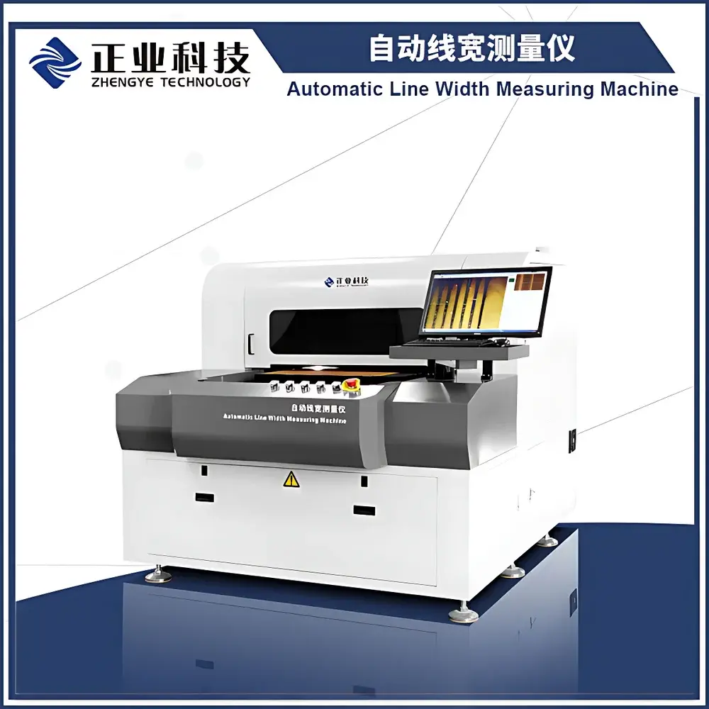
Zhengye ZX-LW Series Online Line Width Inspection System
| Brand | Zhengye |
|---|---|
| Origin | Guangdong, China |
| Manufacturer Type | Manufacturer |
| Country of Origin | China |
| Model | ZX-LW |
| Pricing | Available Upon Request |
Overview
The Zhengye ZX-LW Series Online Line Width Inspection System is a high-precision optical metrology instrument engineered for real-time, non-contact dimensional analysis of micro-scale conductive features in semiconductor and advanced PCB manufacturing processes. It operates on the principle of high-resolution digital microscopy combined with sub-pixel edge detection algorithms, enabling quantitative measurement of critical lithographic parameters—including line width (CD), line spacing, edge roughness, hole-to-line distance, circular/oval aperture diameters, and arc radius—directly on wafers, photomasks, thin-film substrates, and printed circuit boards. Designed for integration into inline process monitoring workflows, the system supports inspection prior to solder mask application (i.e., post-etch, pre-soldermask) and is compatible with both rigid and flexible substrates used in IC packaging, display (LCD/OLED), and high-density interconnect (HDI) PCB production. Its architecture emphasizes stability under factory environmental conditions, including controlled vibration isolation and thermal drift compensation.
Key Features
- Sub-pixel resolution edge detection: Utilizes adaptive thresholding and centroid-based interpolation to achieve measurement repeatability better than ±0.15 µm (3σ) on standard test patterns.
- Precision mechanical focusing stage: Motorized Z-axis with closed-loop feedback ensures consistent focus depth across varying substrate topographies and thicknesses (up to 3.2 mm).
- Integrated red LED alignment illumination: Provides rapid visual registration and operator-guided field-of-view positioning without UV exposure or thermal loading.
- Automated feature recognition engine: Identifies and classifies lines, gaps, vias, blind microvias, and curved contours using morphology-aware pattern matching—eliminating manual ROI selection for routine inspections.
- Real-time SPC dashboard: Embedded statistical process control module calculates Cpk, Cp, X-bar/R charts, and trend alerts per lot, wafer, or die; data export supports CSV, XML, and SECS/GEM protocol for MES integration.
- Modular optical path design: Supports interchangeable objectives (5×–50× magnification) and optional telecentric lenses to minimize perspective distortion during high-magnification CD metrology.
Sample Compatibility & Compliance
The ZX-LW system accommodates substrates ranging from 4″ to 12″ wafers, 610 mm × 610 mm PCB panels, and flat-panel display glass up to 1.1 m × 1.3 m. It accepts standard SEMI E10-compliant cassette loaders and integrates with automated material handling systems via RS-232, Ethernet/IP, and Modbus TCP interfaces. All measurement protocols adhere to ISO 13565-3 (surface texture characterization), ASTM E2857 (line width measurement uncertainty), and IPC-6012/6016 specifications for printed board qualification. The system’s calibration traceability follows NIST-traceable standards through certified reference gratings and step-height standards, and its audit trail functionality satisfies GLP and GMP documentation requirements per FDA 21 CFR Part 11 when configured with user authentication and electronic signature modules.
Software & Data Management
Control and analysis are executed via the proprietary ZX-Insight™ software suite, built on a Windows 10 IoT Enterprise platform. The interface supports multi-user role-based access control (RBAC), version-controlled recipe management, and configurable pass/fail criteria per feature type. Measurement data—including raw images, coordinate metadata, edge profiles, and SPC metrics—is stored in an embedded SQLite database with optional synchronization to SQL Server or Oracle enterprise databases. Raw image archives are retained in lossless TIFF format with EXIF metadata embedding (exposure time, magnification, lens ID, timestamp). Software updates are delivered via secure HTTPS with SHA-256 signature verification, and all data exports include embedded digital signatures compliant with IEC 62443-3-3 cybersecurity guidelines.
Applications
- Post-etch critical dimension verification on PCB inner/outer layers before solder mask lamination
- Photomask defect review and CD uniformity mapping across reticle fields
- Thin-film transistor (TFT) array line width and pitch validation in LCD/OLED backplane fabrication
- IC redistribution layer (RDL) and fan-out wafer-level packaging (FOWLP) metrology
- Microvia diameter and annular ring integrity assessment in HDI and SiP substrates
- Process window qualification for dry etch, plating, and lithography steps in pilot-line development
FAQ
What is the minimum measurable line width supported by the ZX-LW system?
The system achieves reliable detection down to 5 µm line width at 50× magnification with telecentric optics; resolution is scalable with objective selection and lighting configuration.
Does the system support automated defect classification?
Yes—it distinguishes between systematic CD deviations (e.g., etch bias, resist flow) and random defects (e.g., bridging, open circuits) using rule-based classifiers trained on IPC-A-600 and JEDEC JESD22-A108 datasets.
Can the ZX-LW be integrated into a Smart Factory environment?
It supports Industry 4.0 readiness through OPC UA server implementation, MQTT telemetry publishing, and native compatibility with Siemens MindSphere and Rockwell FactoryTalk platforms.
Is calibration required before each inspection run?
No—systematic calibration is performed during startup using onboard reference targets; periodic verification (daily or per shift) is recommended per internal SOPs aligned with ISO/IEC 17025.
What file formats can measurement reports be exported to?
Reports generate in PDF/A-2b (archival), XLSX (SPC-ready), and JSON (API ingestion); custom templates are editable via built-in report designer.


