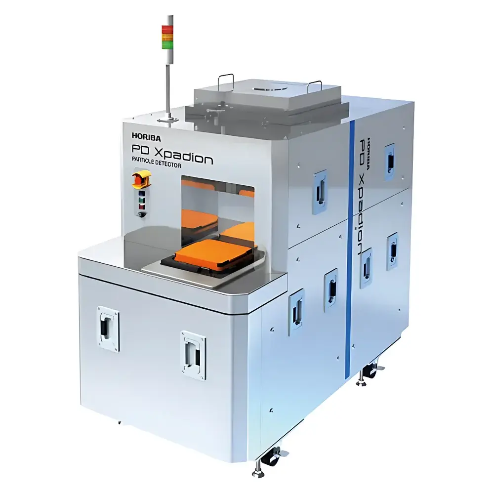
HORIBA PD-Xpadion Photomask Defect Inspection System
| Brand | HORIBA |
|---|---|
| Origin | Japan |
| Manufacturer Type | Original Equipment Manufacturer (OEM) |
| Product Category | Imported |
| Model | PD-Xpadion |
| Pricing | Available Upon Request |
| Particle Detection Sensitivity | 0.5 µm (standard), 0.35 µm (optional), 0.1 µm (with RP-1 integration) |
| Throughput | 12 min per mask (front + back side scan) |
| Mask Size Compatibility | 5-inch to 9-inch |
| Uptime | ≥98% |
| MTBF | 1500 hours |
| Scan Surfaces | Glass substrate, thin-film layer, and patterned side (3-sided inspection) |
| Scan Time per Side | ≤4 minutes |
| Automation Interface | OHT, EFEM, SECS/GEM compliant |
| Optional Modules | Raman-based particle characterization, film thickness & uniformity mapping, film health monitoring, integrated particle removal (RP-1 system) |
Overview
The HORIBA PD-Xpadion Photomask Defect Inspection System is an advanced, platform-based metrology instrument engineered specifically for high-precision defect detection in photomasks and reticles used in advanced lithography nodes (≤7 nm logic and sub-16 nm DRAM). Operating on the principle of bright-field and dark-field scattered-light imaging with multi-angle illumination and polarization-resolved detection, the PD-Xpadion delivers quantitative, repeatable identification of both printable and non-printable defects—including particles, pits, pinholes, bridging, and residual chrome—across all three critical surfaces of a photomask: the quartz substrate (glass side), the absorber or phase-shift film layer, and the patterned top surface. Its optical architecture integrates high-numerical-aperture objectives, stabilized laser sources, and low-noise sCMOS imaging sensors to achieve sub-0.5 µm defect resolution while maintaining high signal-to-noise ratio across diverse film stacks (Cr, MoSi, TaN, and EUV multilayer blanks). Designed for integration into 300 mm and advanced 450 mm fab environments, the system meets stringent requirements for tool stability, environmental control (Class 1 cleanroom compatible), and process traceability under semiconductor manufacturing quality frameworks.
Key Features
- Triple-surface scanning capability: Simultaneous or sequential inspection of glass substrate, thin-film layer, and patterned surface—enabling comprehensive defect root-cause analysis without manual repositioning.
- High-throughput inspection: ≤4 minutes per surface; full front-and-back inspection completed in ≤12 minutes per mask (5″–9″), supporting high-volume mask shop throughput.
- Modular expandability: Native support for field-upgradable modules including Raman spectroscopy for chemical identification of contaminant particles, spectral ellipsometry for film thickness and uniformity mapping (±0.2 nm repeatability), and real-time film stress/oxidation monitoring via in-situ reflectance tracking.
- Robust mechanical architecture: MTBF exceeding 1500 hours; >98% scheduled uptime verified under continuous 24/7 operation in production fabs; vibration-damped granite base and air-isolated motion stages ensure positional stability <±50 nm over 8-hour runs.
- Fab-ready automation: Fully compliant with SEMI E40 (SECS/GEM), E87 (Carrier Handoff), and E157 (Defect Data Collection) standards; direct integration with OHT, EFEM, and AMHS via standard robotic interface protocols.
- Adaptive false-positive suppression: Proprietary classification engine combines morphology-based filtering, multi-spectral intensity profiling, and context-aware pattern recognition to reduce nuisance alarms by >92% versus conventional threshold-based algorithms.
Sample Compatibility & Compliance
The PD-Xpadion accommodates standard photomask formats from 5-inch (127 mm) to 9-inch (229 mm), including square and rectangular blanks with frameless or framed configurations. It supports industry-standard mask carriers from ASML, Nikon, Canon, and Dainippon Screen, as well as custom FOUPs and SMIF pods with mechanical alignment pins and RFID tagging. All handling mechanisms conform to SEMI F47 (Mask Carrier Safety) and F71 (Photomask Handling Requirements). The system complies with ISO 14644-1 Class 1 cleanroom operational limits, IEC 61000-6-2/6-4 EMC standards, and UL 61010-1 safety certification. For regulated environments, audit trail functionality—including user action logging, parameter change history, and raw image metadata—supports FDA 21 CFR Part 11 and EU Annex 11 compliance when deployed with validated software configuration.
Software & Data Management
Powered by HORIBA’s proprietary MaskInsight™ software suite, the PD-Xpadion provides unified control, defect review, classification, and statistical process control (SPC) analytics. The software features a GDSII-aware coordinate registration engine that aligns detected defects directly to layout data for automated printability assessment using rule-based and model-based OPC proximity checks. All inspection logs, classified defect images, and metrology results are stored in a relational database compliant with SQL Server 2019 or Oracle 19c, with optional integration into factory-wide MES (e.g., Applied Materials EnduraLink, PDF Solutions Exensio) via ODBC or RESTful API. Data export supports SEMI E142 (XML-based defect data exchange) and ASTM E2994 (photomask metrology reporting) formats. Full version-controlled software deployment, electronic signatures, and role-based access control (RBAC) are available for GLP/GMP-aligned mask qualification workflows.
Applications
- Front-end mask qualification for EUV and DUV lithography processes at foundry and IDM mask shops.
- In-line monitoring of blank cleaning efficacy and post-etch defectivity during mask fabrication.
- Root-cause analysis of yield-limiting defects through correlative inspection (optical + Raman + ellipsometry).
- Process window qualification for new film stacks (e.g., high-k absorbers, ultra-thin Cr variants) and etch chemistries.
- Support of mask repair verification and post-repair cleanliness validation per ITRS and JEDEC JESD22-A108 standards.
- Integration with HORIBA RP-1 particle removal station for closed-loop defect mitigation—enabling automated “detect → classify → remove → re-inspect” sequences.
FAQ
What defect sizes can the PD-Xpadion reliably detect?
The system achieves a base sensitivity of 0.5 µm on all three mask surfaces under standard operating conditions. With optional high-resolution optics and the RP-1 particle removal module, detection down to 0.1 µm is attainable on flat film regions.
Does the PD-Xpadion support automated defect review with SEM or AFM correlation?
Yes—via standardized coordinate output (GDSII offset + stage position), the system enables seamless handoff to KLA eDR7280, Hitachi CG630, or Park Systems XE7 scanning probe platforms using SEMI E142-compliant review scripts.
Can the PD-Xpadion be retrofitted with new modules after initial installation?
All hardware interfaces—including optical bays, sensor ports, and vacuum feedthroughs—are designed for field upgradeability. Module installation requires only mechanical mounting, electrical interlock verification, and software license activation—no structural modification needed.
Is remote diagnostics and predictive maintenance supported?
Yes—the system includes embedded telemetry (vibration, thermal drift, laser power, stage encoder feedback) streamed to HORIBA’s cloud-based Predictive Service Platform (PSP), enabling failure mode forecasting and proactive spare-part provisioning.
How is calibration traceability maintained?
Each system ships with NIST-traceable calibration artifacts (PSL sphere arrays, step-height standards) and automated daily self-calibration routines validated against ISO/IEC 17025-accredited procedures performed at HORIBA’s Tokyo Metrology Center.


