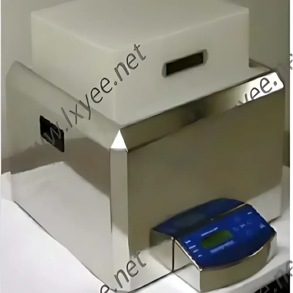

Nano-Master SWC-3000 Megasonic Wafer and Photomask Cleaning System
| Brand | Nano-Master |
|---|---|
| Origin | Germany |
| Model | SWC-3000 |
| Maximum Substrate Size | 300 mm (12") round or 230 mm × 230 mm (9" × 9") square |
| Control System | Microprocessor-based automation |
| Optional Modules | PVA brush station, Chemical Dispense Unit (CDU), N₂ ionizer, IR drying lamp, custom photomask/wafer chucks |
Overview
The Nano-Master SWC-3000 is a benchtop megasonic cleaning system engineered for high-precision, non-destructive removal of sub-100 nm particulates, organic residues, and native oxides from semiconductor wafers and photomasks. It operates on the principle of megasonic energy transmission—typically at 1 MHz—generating controlled acoustic streaming and micro-cavitation in deionized water or process-compatible chemistries without inducing surface damage. Unlike ultrasonic cleaning, which relies on aggressive cavitation collapse, megasonic excitation produces laminar fluid motion that dislodges contaminants via shear forces while preserving delicate topographies such as sub-10 nm line/space patterns, EUV multilayer stacks, and low-k dielectric films. The SWC-3000 integrates cleaning, chemical treatment, mechanical brushing, and spin-drying into a single, programmable process sequence—enabling full traceability and reproducibility across R&D, pilot-line, and low-volume production environments.
Key Features
- Benchtop footprint with integrated megasonic transducer array optimized for uniform energy distribution across 300 mm wafers or 230 mm × 230 mm photomasks
- Microprocessor-controlled process sequencing with up to 99 user-defined recipes, each supporting independent timing, power ramping, rotation speed (0–2000 rpm), and fluid delivery parameters
- Non-contact megasonic cleaning mode operating at fixed 1 MHz frequency with adjustable power density (0–15 W/cm²) to prevent device-level erosion on patterned GaAs, InP, Ge, and Si substrates
- Integrated spin-rinse-dry (SRD) module with IR-assisted drying option for residue-free moisture removal post-cleaning
- Modular architecture supporting optional PVA brush station for localized mechanical scrubbing, Chemical Dispense Unit (CDU) for sequential or simultaneous reagent delivery (e.g., SC1, SC2, dilute HF), and N₂ ionizer for static charge mitigation during handling
- Compliant with SEMI S2/S8 safety standards; all wet process zones constructed from perfluoroalkoxy (PFA)-lined stainless steel and quartz components to ensure chemical inertness and particle-free operation
Sample Compatibility & Compliance
The SWC-3000 accommodates bare and patterned substrates including silicon, fused silica, CaF₂, and quartz photomasks; EUV mask blanks with Ru-capped Mo/Si multilayers; X-ray masks with Ta/Ni absorbers; and display-grade ITO-coated glass panels. It supports post-CMP wafer cleaning where slurry residue removal must avoid scratching soft Cu/low-k interconnects, and post-plasma etch or photoresist ash residue removal without undercutting sub-20 nm features. All process parameters—including megasonic dwell time, chemical exposure duration, and spin acceleration profile—are logged with timestamp and operator ID, satisfying GLP/GMP documentation requirements and enabling audit-ready compliance with ISO 9001, ISO 14644-1 Class 5 cleanroom integration, and FDA 21 CFR Part 11 electronic record integrity protocols when paired with validated software configurations.
Software & Data Management
The embedded control interface provides real-time monitoring of transducer impedance, bath temperature (±0.2 °C), rotational velocity, and fluid flow rates. Process logs are exportable in CSV format with metadata fields compliant with ASTM F2217-21 (Standard Guide for Semiconductor Equipment Data Collection). Optional Ethernet/IP connectivity enables remote diagnostics and integration into factory MES systems via SECS/GEM protocol support. Audit trails include full revision history of recipe modifications, user login/logout events, and alarm-triggered data snapshots—ensuring alignment with quality management systems requiring ALCOA+ (Attributable, Legible, Contemporaneous, Original, Accurate, Complete, Consistent, Enduring, Available) data integrity principles.
Applications
- Cleaning of EUV and deep-UV photomasks prior to inspection or exposure
- Removal of CMP slurry particles from 300 mm logic and memory wafers
- Post-etch residue clearance from III-V compound semiconductor devices (GaAs HBTs, InP photonics)
- Pre-bonding surface preparation for direct wafer bonding and TSV processing
- Residue-free cleaning of diced die mounted on frame tape, including those with fragile under-bump metallization
- Megasonically assisted photoresist or hardmask lift-off on high-aspect-ratio structures
- Cleaning of optical components (lenses, mirrors, beam splitters) used in lithography tools and metrology platforms
FAQ
What substrate sizes does the SWC-3000 support?
The system handles circular wafers up to 300 mm (12 inches) in diameter and square substrates up to 230 mm × 230 mm (9 inches × 9 inches), including photomasks, reticles, and flat-panel display substrates.
Is the megasonic energy adjustable in frequency?
No—the SWC-3000 operates exclusively at 1 MHz, a frequency selected to maximize acoustic streaming efficiency while minimizing cavitation-induced surface damage on advanced node devices.
Can the system be integrated into a Class 1 cleanroom environment?
Yes. The SWC-3000 meets SEMI S2 electrical safety and S8 ergonomic requirements and is compatible with ISO 14644-1 Class 1–5 environments when installed with appropriate exhaust and DI water supply infrastructure.
Does the system support automated chemical replenishment?
Chemical delivery is programmable via the optional Chemical Dispense Unit (CDU), but closed-loop concentration monitoring and auto-replenishment require external integration with third-party conductivity/pH sensors and dosing pumps.
What certifications does the SWC-3000 carry?
The system is CE-marked and complies with IEC 61000-6-2 (immunity) and IEC 61000-6-4 (emissions); full regulatory documentation—including RoHS and REACH declarations—is available upon request for qualification in regulated manufacturing sites.


