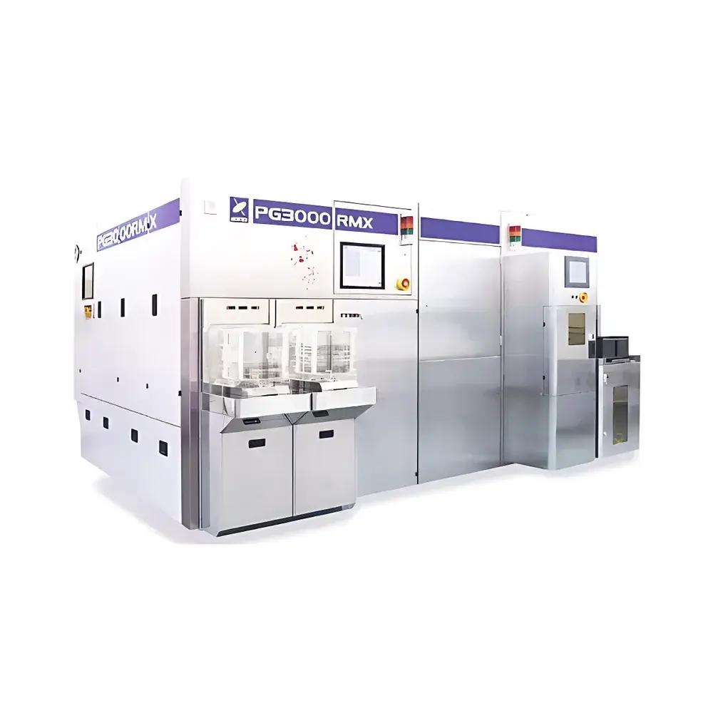
ACCRETECH PG3000RMX Wafer Grinding and Polishing System
| Brand | ACCRETECH (Tokyo Seimitsu) |
|---|---|
| Origin | Japan |
| Model | PG3000RMX |
| Type | Integrated Backside Grinding & CMP Stress-Relief System for Ultra-Thin Wafer Processing |
| Application | Front-End Wafer Preparation for 15 µm Final Thickness Production |
Overview
The ACCRETECH PG3000RMX is a fully integrated, high-precision wafer backgrinding and stress-relief polishing system engineered for front-end semiconductor manufacturing of ultra-thin silicon wafers. Designed to meet the stringent dimensional and surface integrity requirements of advanced packaging (e.g., TSV, Fan-Out WLP, 3D IC stacking), the PG3000RMX employs dual-stage precision grinding followed by chemical-mechanical polishing (CMP)-compatible stress relief to achieve final wafer thicknesses down to 15 µm with sub-micron total thickness variation (TTV) and nanometer-level surface roughness (Ra < 0.5 nm). Unlike conventional single-stage grinders, the PG3000RMX incorporates a proprietary rigid chucking architecture with full-wafer vacuum support and real-time in-situ thickness monitoring via non-contact eddy-current sensors—enabling closed-loop thickness control throughout the entire process sequence. The system operates under Class 100 cleanroom-compatible environmental controls and supports 200 mm and 300 mm diameter wafers with patterned device layers protected by temporary bonding films (e.g., UV-curable or thermal-release tapes).
Key Features
- Dual-stage grinding module: Coarse grinding (diamond wheel, adjustable feed rate) followed by fine grinding (resin-bond diamond wheel) for controlled material removal and minimized subsurface damage.
- Integrated stress-relief polishing station: Equipped with low-pressure, low-abrasive CMP head and programmable slurry delivery for post-grind mechanical stress mitigation without delamination risk.
- RM (Release Module) integration: Automated wafer unloading directly onto dicing frames using frame-mounted adhesive tape handling—eliminating manual transfer and reducing chipping/cracking at ultra-thin geometries.
- Real-time metrology feedback loop: In-process eddy-current thickness measurement with ±0.2 µm repeatability; synchronized with grinding wheel dressing cycles and feed compensation algorithms.
- Process traceability architecture: Full audit trail logging compliant with ISO 9001 and SEMI E10/E142 standards; supports GLP/GMP-aligned electronic batch records.
- Modular tooling interface: Compatible with standard SEMI-compliant FOUPs and EFEM integration for automated fab line deployment.
Sample Compatibility & Compliance
The PG3000RMX accommodates silicon wafers (Si, SiC, GaN-on-Si), SOI substrates, and compound semiconductor wafers up to 300 mm in diameter. It is qualified for use with temporary bonding systems including DVS, TAIKO, and carrier-based thinning processes. All wet modules comply with SEMI F57 (chemical resistance) and F61 (slurry containment) specifications. Mechanical safety conforms to ISO 13857 and IEC 60204-1; electrical design meets CE and UL 61010-1 requirements. The system supports validation documentation packages aligned with FDA 21 CFR Part 11 for electronic signatures and data integrity in regulated environments.
Software & Data Management
Controlled by ACCRETECH’s proprietary GRIND-OS™ platform, the PG3000RMX features a deterministic real-time operating system (RTOS) with deterministic motion control loops (≤1 ms cycle time). Recipe management includes multi-layer parameter sets for grinding depth, wheel speed (50–500 rpm), table feed rate (0.1–5 µm/sec), and polishing pressure (0.5–3.0 psi). All process data—including sensor logs, motor current traces, and thickness profiles—are stored in SQLite-based local databases with optional OPC UA server export for MES/SCADA integration. Audit trails include user authentication, timestamped parameter changes, and electronic signature capture per ASTM E2500-13 guidelines.
Applications
- Production-scale thinning of 300 mm logic and memory wafers to 15–25 µm for 3D NAND and HBM stack integration.
- Backgrinding of image sensor wafers (CIS) with high-aspect-ratio micro-lenses requiring minimal warp and TTV < 0.8 µm.
- Pre-CMP conditioning for copper damascene wafers prior to electrochemical planarization.
- Stress-balanced thinning of SiC power device wafers to enable high-voltage die singulation with reduced chipping.
- Research-grade thinning of novel 2D material heterostructures (e.g., MoS₂/graphene on Si) using low-damage grinding protocols.
FAQ
What wafer diameters does the PG3000RMX support?
The system is configured for 200 mm and 300 mm wafers with interchangeable chucks and alignment modules.
Does the PG3000RMX include in-line thickness metrology?
Yes—integrated non-contact eddy-current sensors provide real-time thickness feedback with ≤0.2 µm repeatability and automatic feed compensation.
Is the RM (Release Module) a factory-installed option or field-upgradable?
The RM is a factory-integrated subsystem; it cannot be retrofitted post-delivery due to mechanical synchronization requirements with the grinding spindle and frame-handling robotics.
Can the PG3000RMX process wafers with through-silicon vias (TSVs)?
Yes—its low-stress grinding and stress-relief polishing sequence has been validated for TSV wafers up to 50 µm thick with < 0.3% via tilt distortion.
What level of process documentation is provided for IQ/OQ/PQ qualification?
ACCRETECH supplies a complete GxP-ready validation package including URS, FDS, SDS, FAT/SAT reports, and traceable calibration certificates per ISO/IEC 17025-accredited labs.


