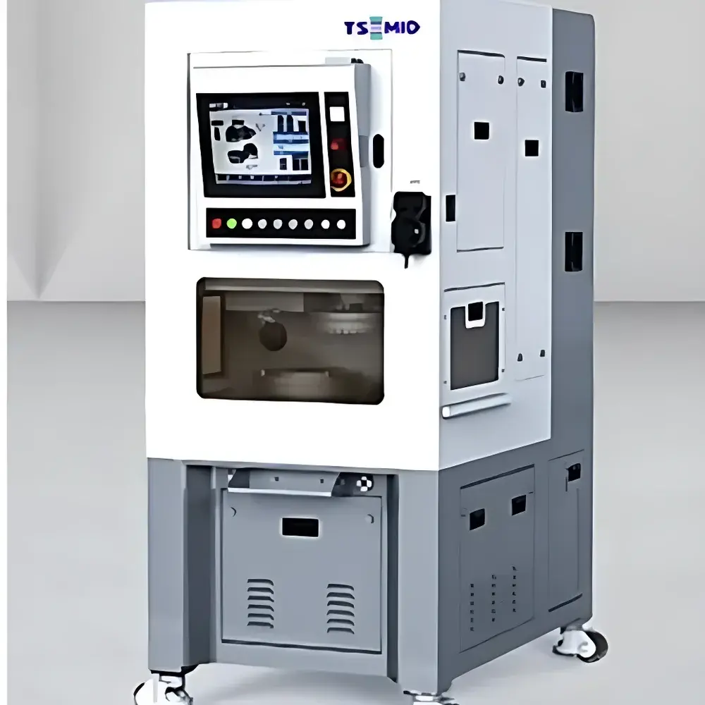
TSD IVG Series Semi-Automatic Dual-Axis Wafer Thinning Machine
| Brand | TSD |
|---|---|
| Model | IVG Series |
| Origin | Beijing, China |
| Type | Semi-Automatic Dual-Axis Wafer Thinning System |
| Maximum Wafer Size | 200 mm (IVG-2020) / 300 mm (IVG-3020) |
| Grinding Wheel OD | 203 mm / 303 mm |
| Spindle Power | 6.0 kW / 9.5 kW |
| Spindle Speed | 0–6000 rpm / 0–4000 rpm |
| Chuck Rotation Speed | 0–380 rpm |
| Z-Axis Feed Rate | 0.1–1000 µm/sec |
| In-Line Thickness Measurement Range | 0–4800 µm |
| Thickness Repeatability | ±1 µm |
| Non-Contact Gauging (NCG) | Optional |
Overview
The TSD IVG Series Semi-Automatic Dual-Axis Wafer Thinning Machine is a precision grinding system engineered for controlled material removal from semiconductor wafers, optical substrates, and advanced thin-film materials. It operates on the principle of precision lapping and fine-grit mechanical grinding using two independently driven spindles—enabling simultaneous coarse and fine grinding stages within a single setup. This dual-axis architecture minimizes inter-process handling, reduces thermal drift between operations, and improves thickness uniformity across the wafer surface. Designed for front-end and back-end semiconductor fabrication environments, the IVG platform supports post-bonded wafer thinning, temporary bonding/debonding workflows, and high-aspect-ratio substrate preparation where sub-micron thickness control and nanometer-level surface integrity are critical.
Key Features
- Dual-spindle configuration with independent speed and feed control—optimized for sequential roughing and finishing passes without manual repositioning.
- Integrated in-line optical micrometer module (OMM) with real-time thickness feedback and closed-loop compensation—ensuring repeatability of ±1 µm across full wafer maps.
- Modular chuck design supporting vacuum-based fixation of silicon, sapphire, SiC, GaAs, and glass wafers up to 300 mm diameter; compatible with standard carrier frames and adhesive tapes per JEDEC JEP161 and SEMI standards.
- Z-axis motion system with linear encoder feedback and sub-micron positioning resolution (0.1 µm minimum incremental feed), enabling precise depth-of-cut control during step-and-repeat or continuous-feed grinding modes.
- Programmable process recipes stored locally with timestamped audit logs—supporting GLP-compliant documentation requirements for R&D and pilot-line validation.
- Open I/O architecture permitting integration with factory automation systems (SECS/GEM) and third-party metrology tools via Ethernet/IP or Modbus TCP protocols.
Sample Compatibility & Compliance
The IVG series accommodates rigid and semi-rigid substrates ranging from 100 mm to 300 mm in diameter, including but not limited to monocrystalline silicon, fused silica, lithium niobate, and polymer-supported ultra-thin films. All mechanical interfaces conform to SEMI E10 (Specification for Definition and Measurement of Equipment Reliability and Maintainability) and SEMI E172 (Wafer Backside Grinding Interface Requirements). The OMM-based thickness monitoring subsystem complies with ISO 14284:2021 for non-contact dimensional metrology of planar substrates. Optional NCG modules meet ASTM F3012-15 guidelines for non-destructive thickness verification of bonded wafers prior to dicing.
Software & Data Management
The embedded HMI runs on a real-time Linux OS with deterministic motion control firmware. Process parameters—including spindle RPM, chuck rotation, Z-feed profile, coolant flow rate, and OMM trigger thresholds—are configurable via intuitive graphical interface. Each run generates a structured CSV log file containing time-stamped thickness readings, axis positions, power consumption traces, and alarm history. Data export supports USB storage and network transfer (SFTP/SCP), with optional add-on modules enabling 21 CFR Part 11 compliance through electronic signatures, role-based access control, and immutable audit trails.
Applications
- Semiconductor backend processing: Backgrinding of 3D IC stacks, TSV-exposed wafers, and fan-out wafer-level packages (FOWLP) requiring final thicknesses between 25–150 µm.
- MEMS and sensor fabrication: Controlled thinning of SOI wafers to define device layer thickness while preserving buried oxide integrity.
- Optoelectronic component manufacturing: Precision thickness tuning of laser diode substrates and photonic integrated circuit (PIC) platforms to meet waveguide dispersion targets.
- Research and development labs: Rapid prototyping of ultra-thin membranes for flexible electronics, 2D material transfer substrates, and quantum device test vehicles.
- Compound semiconductor processing: Low-damage grinding of GaN-on-silicon and SiC power devices where subsurface damage layer depth must remain below 200 nm.
FAQ
What wafer diameters does the IVG series support?
The IVG-2020 model accommodates wafers up to 200 mm (8-inch), while the IVG-3020 supports up to 300 mm (12-inch) substrates with appropriate chuck configuration.
Is the non-contact gauging (NCG) system included by default?
NCG is an optional upgrade; the base configuration includes the optical micrometer module (OMM) with contactless laser triangulation measurement over the full 0–4800 µm range.
Can the machine be integrated into an automated fab environment?
Yes—the system provides native SECS/GEM communication capability and supports host-directed recipe loading, status polling, and event reporting via standard semiconductor equipment connectivity protocols.
What level of surface roughness can be achieved after thinning?
With optimized wheel selection and process tuning, typical post-grind Ra values range from 0.8–2.5 nm on silicon wafers, depending on final thickness and material hardness.
Does the system comply with cleanroom class requirements?
The IVG platform meets ISO Class 5 (Class 100) cleanroom compatibility when operated with HEPA-filtered coolant recirculation and sealed bearing housings; full qualification reports available upon request.


