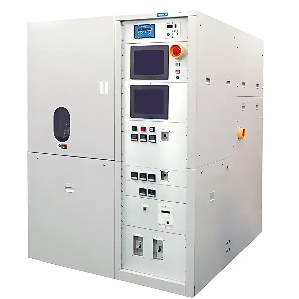
SAMCO PD-100ST Plasma-Enhanced Chemical Vapor Deposition System
| Brand | SAMCO |
|---|---|
| Origin | Japan |
| Model | PD-100ST |
| Substrate Diameter | Ø100 mm (4") |
| Deposition Temperature Range | 80–400 °C |
| SiO₂ Deposition Rate | >300 nm/min |
| Maximum Film Thickness | Up to 100 µm |
| Deposition Technology | Liquid-source PECVD with RF self-bias coupling |
| Precursor Type | Liquid TEOS (tetraethyl orthosilicate), optional Ge/P/B dopant sources |
| Stress Control | Low-stress SiO₂ via self-bias tuning |
| Step Coverage | High-aspect-ratio conformality |
| Footprint | Compact, cleanroom space-optimized |
Overview
The SAMCO PD-100ST is a research-grade plasma-enhanced chemical vapor deposition (PECVD) system engineered for low-temperature, high-rate thin-film synthesis on temperature-sensitive and geometrically complex substrates. Unlike conventional thermal CVD systems, the PD-100ST employs radiofrequency (RF) capacitively coupled plasma with integrated self-bias control to dissociate precursor vapors—primarily liquid TEOS—under non-equilibrium conditions. This enables robust film growth at substrate temperatures as low as 80 °C, making it uniquely suitable for polymer substrates (e.g., polyimide, PET, COC), flexible electronics, and 3D-integrated structures where thermal budget constraints prohibit conventional processing. The system operates in a controlled vacuum environment (<10⁻² Pa base pressure) with precise mass flow and RF power regulation (13.56 MHz), ensuring repeatable stoichiometry, refractive index tunability (via Ge/P/B co-injection), and intrinsic stress management through bias voltage modulation.
Key Features
- Compact, modular architecture optimized for Class 100–1000 cleanroom integration—requires only ~1.2 m² floor space.
- Ø100 mm (4-inch) substrate compatibility with manual or semi-automated load-lock option.
- RF-driven self-bias deposition technology enabling low-stress (<50 MPa compressive/tensile), high-density SiO₂ films without post-annealing.
- Liquid precursor delivery system with integrated vaporizer and pressure-controlled injection—eliminates cylinder-based gas handling and improves repeatability for TEOS, germanium tetraethoxide (GTEOS), phosphoric acid esters, and boric acid derivatives.
- Real-time process monitoring via optical emission spectroscopy (OES) port and integrated vacuum gauges (capacitance manometer + Pirani).
- Programmable recipe storage (≥100 profiles) with timestamped parameter logging compliant with GLP audit requirements.
Sample Compatibility & Compliance
The PD-100ST accommodates rigid and flexible substrates including silicon wafers, glass, quartz, alumina, polyimide foils, and molded plastic components. Its low-temperature capability supports direct deposition onto micro-optical waveguides, MEMS cantilevers, and through-silicon vias (TSVs) in 3D-LSI packages—achieving uniform step coverage (>90% at aspect ratios ≥10:1). All wetted materials comply with SEMI F57 standards for semiconductor tool construction. Vacuum chamber and gas lines are electropolished stainless steel (316L) with VCR fittings; O-rings meet USP Class VI biocompatibility requirements. The system meets CE machinery directive (2006/42/EC), EMC directive (2014/30/EU), and is compatible with ISO 9001-certified fabrication workflows.
Software & Data Management
Control is executed via a Windows-based HMI with deterministic real-time kernel, supporting dual-language UI (English/Japanese) and role-based access control (operator, engineer, administrator). Process data—including RF forward/reflected power, chamber pressure, substrate temperature, precursor flow rates, and OES intensity traces—are logged at 100 Hz resolution and exported in CSV or HDF5 format. Audit trail functionality satisfies FDA 21 CFR Part 11 requirements: all parameter changes, user logins, and alarm events are digitally signed and time-stamped with immutable records. Optional integration with factory MES via SECS/GEM protocol enables traceability from wafer ID to film thickness map.
Applications
- Deposition of stress-engineered SiO₂ passivation and encapsulation layers on flexible OLED backplanes and bio-sensor substrates.
- Conformal insulation of high-aspect-ratio TSV sidewalls in 2.5D/3D IC packaging.
- Growth of graded-index silica cladding and core layers for planar lightwave circuits (PLCs) and silicon photonics waveguides.
- Fabrication of etch masks for deep reactive ion etching (DRIE) in MEMS device release processes.
- Deposition of temperature-compensating films (e.g., BPSG, PSG) on surface acoustic wave (SAW) resonators for telecom and IoT timing devices.
- Low-k dielectric integration on organic interposers and fan-out wafer-level packaging (FOWLP) substrates.
FAQ
What substrates can be processed in the PD-100ST?
Standard configurations support Ø100 mm wafers and flat substrates up to 100 × 100 mm; custom chucks accommodate irregular shapes and flexible foils.
Is the system compatible with hazardous precursors?
Yes—the liquid delivery module includes leak-tight vaporization chambers, secondary containment, and integrated abatement interface for acidic or pyrophoric precursors per SEMI S2/S8 guidelines.
Can film stress be actively tuned during deposition?
Yes—via real-time adjustment of RF self-bias voltage (±500 V range), which directly modulates ion energy and network cross-linking density in growing SiO₂.
Does the system support in-situ thickness monitoring?
Optional ellipsometry or laser interferometry ports are available; ex-situ metrology integration (e.g., with Sentech SE 850) is supported via digital I/O and TCP/IP.
What maintenance intervals are recommended?
Chamber cleaning every 50 runs; RF matching network calibration quarterly; liquid precursor filters replaced every 200 hours of operation—logbook templates provided per ISO/IEC 17025 documentation standards.


