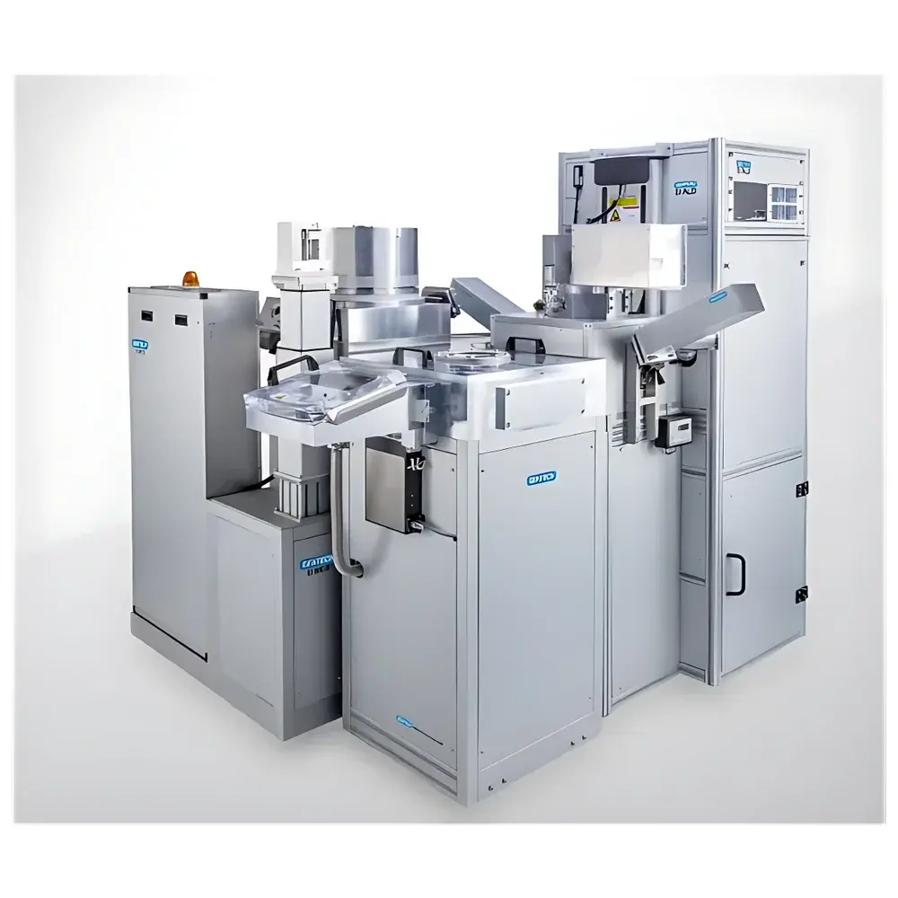
SENTECH Plasma Etching Cluster System
| Brand | SENTECH |
|---|---|
| Origin | Germany |
| Manufacturer Type | Authorized Distributor |
| Origin Category | Imported |
| Model | SENTTECH Cluster System |
| Price | Upon Request |
Overview
The SENTECH Plasma Etching Cluster System is a modular, ultra-high-vacuum (UHV)-compatible semiconductor process platform engineered for precision plasma etching and thin-film deposition in R&D and pilot-line manufacturing environments. Built upon a robust load-lock architecture, the system integrates one or more process modules—including inductively coupled plasma (ICP) etchers, reactive ion etchers (RIE), atomic layer deposition (ALD), and inductively coupled plasma-enhanced chemical vapor deposition (ICP-ECVD)—with a central transfer chamber equipped with a high-precision robotic handler. The system operates under base pressures down to 1×10⁻⁸ mbar, ensuring minimal contamination and enabling reproducible surface chemistry control critical for advanced node development (e.g., sub-28 nm gate patterning, MEMS release, and compound semiconductor processing). Its design adheres to SEMI S2/S8 safety and ergonomics standards and supports integration into cleanroom Class 100 (ISO Class 5) environments.
Key Features
- Modular architecture with 3–6-port transfer chamber, accommodating up to two cassette stations for enhanced throughput and wafer-handling redundancy.
- Integrated six-axis vacuum-compatible robotic arm with ±5 µm positional repeatability and He-backside cooling support for thermal stabilization of wafers up to 200 mm (8-inch) diameter.
- Process module interoperability: seamless integration of ICP etch, RIE, ALD, and ICP-ECVD tools—each independently pumped and controlled via isolated RF/DC/MW power delivery networks.
- Load-lock and/or cassette-based vacuum loading options, with automated pressure ramping and bake-out protocols compliant with SEMI E10 and ISO 14644-1 particulate monitoring requirements.
- Dual-cassette station configuration enables continuous batch loading/unloading, reducing idle time and supporting >95% tool utilization in 24/7 operation.
- Hardware-controlled real-time interlocks for chamber door position, RF match status, gas flow integrity, and cryo-pump temperature—managed by a SIL2-certified PLC per IEC 61508.
Sample Compatibility & Compliance
The system handles substrates from 100 mm (4-inch) to 200 mm (8-inch) silicon, SiC, GaN, sapphire, and quartz wafers—including patterned, bonded, or ultra-thin (<100 µm) substrates. Carrier adaptability is achieved via interchangeable chucks and cassette pitch adapters—no mechanical retrofitting required. All wet-chemical pre/post-process interfaces (e.g., spin-rinse developers or DI water rinse stations) are designed for optional downstream integration per SEMI F47 chemical compatibility guidelines. The platform meets EU Machinery Directive 2006/42/EC, PED 2014/68/EU for vacuum vessels, and complies with FDA 21 CFR Part 11 data integrity requirements when paired with validated SIA software configurations.
Software & Data Management
Control is executed through SENTECH’s SIA (Semiconductor Integration Architecture) software—a client-server application built on Windows Server with OPC UA-compliant device drivers. The system provides full recipe management with version-controlled parameter sets, audit-trail logging (including operator ID, timestamp, and parameter deviations), and electronic signature support aligned with GLP/GMP Annex 11 and ISO 9001:2015 documentation standards. Process data—including RF forward/reflected power, chamber pressure traces, optical emission spectroscopy (OES) intensity profiles, and endpoint detection signals—is streamed at 100 Hz resolution to an embedded SQL database. Raw logs export in HDF5 format for traceable offline analysis using MATLAB, Python (Pandas/HDF5), or JMP.
Applications
- High-selectivity etching of SiO₂, Si₃N₄, and low-k dielectrics using fluorocarbon chemistries (C₄F₈, CHF₃) in ICP mode.
- Anisotropic trench etching for MEMS inertial sensors and RF-SOI devices via pulsed RIE with sub-5 nm CD uniformity (3σ).
- Conformal Al₂O₃ and HfO₂ ALD films for high-k gate stacks, with thickness control <±0.05 nm across 200 mm wafers.
- Plasma-assisted nitridation and surface passivation of GaN HEMT epitaxial layers prior to gate metallization.
- Multi-step process sequences—e.g., etch → ash → clean → deposit—executed without breaking vacuum, minimizing native oxide regrowth.
FAQ
Does the cluster support 300 mm wafer handling?
No—this configuration is optimized for 100–200 mm substrates. SENTECH offers separate 300 mm platforms with larger transfer chambers and extended robotic reach.
Can the system be retrofitted with additional process modules after installation?
Yes—modular flange interfaces (CF100/CF160) and standardized power/data connectors allow field-upgradable expansion with minimal downtime.
Is remote diagnostics and predictive maintenance supported?
Yes—SIA software includes SNMP-based health monitoring, real-time pump oil degradation alerts, and scheduled maintenance flagging based on cumulative RF hours and valve actuation counts.
What level of validation documentation is provided?
Factory acceptance testing (FAT) reports, IQ/OQ protocols, and URS traceability matrices are delivered as part of the standard commissioning package.
Are custom gas delivery manifolds available for corrosive precursors (e.g., ClF₃, WF₆)?
Yes—options include Hastelloy-C276 manifolds, heated VCR fittings, and integrated residual gas analyzers (RGA) with NIST-traceable calibration certificates.


