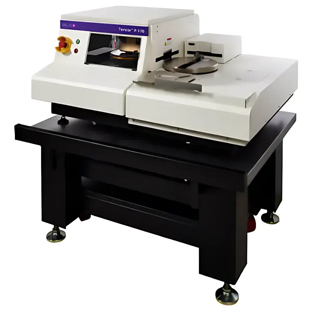
KLA Tencor® P-170 Automated Stylus Profilometer
| Brand | KLA |
|---|---|
| Origin | USA |
| Manufacturer | KLA Corporation |
| Product Type | Imported |
| Model | Tencor® P-170 |
| Measurement Principle | Inductive |
| Vertical Measurement Range | 0.5 nm – 1000 µm |
| Vertical Resolution | Sub-nanometer (typical) |
| Probe Tip Radius | < 12 nm (standard diamond tip) |
| Normal Force Range | 0.03–15 mg (closed-loop force control) |
| Maximum Scan Length | 200 mm (single-pass, no stitching required) |
| Step Height Repeatability | ≤ 0.15 nm (1σ, over 24 h) |
| Maximum Sample Size | Ø200 mm × 25 mm thick |
| Optical System | 5 MP color camera with motorized zoom and dual-view (top + side) optics |
| Automation | Integrated robotic handler for opaque (e.g., Si) and transparent (e.g., sapphire) wafers (Ø75–200 mm) |
| Compliance | ASTM E1399, ISO 4287, ISO 25178-2, USP <1059>, FDA 21 CFR Part 11 (audit trail & electronic signature enabled) |
Overview
The KLA Tencor® P-170 Automated Stylus Profilometer is a production-grade, in-line capable surface metrology system engineered for high-reproducibility 2D and 3D topographic characterization of micro- and nanostructured surfaces. Utilizing inductive displacement sensing with closed-loop, real-time force control, the P-170 maintains consistent mechanical interaction between the stylus and sample across extreme step heights—from sub-nanometer features to 1000 µm steps—without manual recalibration or probe repositioning. Its core architecture integrates a vibration-isolated granite base, ultra-flat air-bearing scanning stage, and UltraLite® sensor platform, delivering metrological stability required for process monitoring in semiconductor front-end, compound semiconductor, MEMS, LED, and advanced packaging environments. Unlike optical profilers limited by coherence or reflectivity constraints, the P-170 provides traceable, direct-contact measurement of true surface height, making it indispensable for quantifying film thickness, etch depth, CMP removal rates, and lithographic resist profiles.
Key Features
- Inductive stylus sensing with sub-nanometer vertical resolution and ≤ 0.15 nm step height repeatability (1σ, 24-hour drift test)
- Dynamic force control (0.03–15 mg range) ensures uniform contact pressure across soft polymers (e.g., photoresist), brittle dielectrics, and hard metals
- 200 mm single-pass scan capability eliminates stitching artifacts and reduces measurement uncertainty in large-area wafer-level analysis
- Dual-axis optical imaging system: 5 MP color camera with motorized zoom, top-view + side-view optics, and integrated arc correction algorithm to compensate for stylus trajectory curvature
- Automated wafer handling: SECS/GEM-compliant robotic arm supports Ø75–200 mm opaque (Si, GaAs) and transparent (sapphire, glass) substrates
- HRP®-260-derived mechanical platform validated in high-volume manufacturing environments for >99.5% uptime and tool-to-tool recipe portability
- Click-to-scan stage control with real-time coordinate mapping enables rapid program setup and feature targeting without scripting
Sample Compatibility & Compliance
The P-170 accommodates rigid and semi-rigid planar substrates up to 200 mm in diameter and 25 mm thick, including silicon, quartz, sapphire, fused silica, and patterned SOI wafers. Its low-force operation enables reliable profiling of delicate structures such as lift-off metal lines, porous low-k dielectrics, and spin-coated organic layers. All measurements adhere to internationally recognized standards: surface roughness parameters follow ISO 4287 and ISO 25178-2; step height reporting conforms to ASTM E1399; and stress calculation utilizes the Stoney equation per ASTM F390. The system supports full GLP/GMP compliance through configurable audit trails, electronic signatures, user access levels, and 21 CFR Part 11–compliant data archiving—critical for qualification in FDA-regulated medical device or automotive semiconductor supply chains.
Software & Data Management
The proprietary VisionX™ software provides an intuitive, workflow-driven interface with drag-and-drop recipe building, real-time waveform visualization, and automated pass/fail decision logic. It includes industry-standard filtering (Gaussian, S-filter, L-filter), leveling algorithms (least-squares, reference line, polynomial), and advanced analysis modules for texture (Sa, Sq, Sz), shape (wafer bow, warp, TTV), stress (2D radial scan + multi-angle 3D reconstruction), and defect metrology (KLARF file import/export, coordinate-based defect navigation). Raw profile data is stored in vendor-neutral ASCII and HDF5 formats. Integration with factory MES systems is achieved via SEMI E30 (GEM) and E40 (SECS-II) protocols, enabling automated job dispatch, result logging, and SPC charting directly from the tool.
Applications
- Step Height Metrology: Quantification of deposition/etch depths in gate stacks, TSVs, redistribution layers, and MEMS release etches (0.5 nm–1000 µm range)
- Surface Texture Analysis: Separation of roughness (Rq, Ra) and waviness (Wq, Wa) per ISO 25178 using configurable spatial filters
- Wafer-Level Shape & Stress: Full-diameter 2D bow/warp mapping and 3D stress reconstruction via multi-angle scanning and Stoney equation implementation
- Film Stress on Curved Substrates: Radius-of-curvature measurement on lens molds, VCSEL substrates, and flexible hybrid electronics
- Defect Topography: KLARF-aligned 2D/3D profiling of scratches, particles, and residue with depth/width/volume quantification
- Process Qualification: In-line monitoring of ALD cycle counts, electroplating thickness uniformity, and CMP endpoint detection
FAQ
What materials can be measured without risk of damage?
The P-170’s closed-loop force control enables safe profiling of photoresists, polyimides, low-k dielectrics, aluminum, copper, and silicon nitride. Diamond-tipped probes (radius <12 nm) are standard; custom tips (e.g., tungsten carbide) are available for abrasive or ultra-hard surfaces.
Does the system support transparent substrates like sapphire or fused silica?
Yes—the dual-view optical system and non-optical stylus sensing eliminate reliance on substrate reflectivity or transparency, ensuring robust autofocus and feature recognition on all common semiconductor and optoelectronic substrates.
How is measurement traceability ensured across multiple tools?
All P-170 systems ship with NIST-traceable step height standards and undergo factory calibration per ISO/IEC 17025. Tool-to-tool correlation is maintained via HRP®-260 mechanical architecture and VisionX™’s standardized analysis pipeline.
Can the P-170 integrate into an automated fab environment?
Yes—it complies fully with SEMI E30 (GEM), E40 (SECS-II), and E148 (equipment self-description) standards and supports dry-run mode for recipe validation prior to live wafer processing.
Is 3D stress mapping supported out of the box?
Yes—3D stress reconstruction is enabled via automated multi-angle scanning sequences and built-in Stoney equation solvers, requiring no third-party post-processing.