Abner ABN-MLM-002 Mask Aligner
| Brand | Abner |
|---|---|
| Origin | Jiangsu, China |
| Model | ABN-MLM-002 |
| Light Source | High-intensity Hg lamp / 365 nm i-line / Optional 405 nm UV LED |
| Illumination Uniformity | ≥90% |
| Intensity Stability | ±2% |
| Intensity Density | ≥50 mW/cm² (at wafer plane) |
| Optical Resolution | ≤2 µm (contact mode), ≤5 µm (proximity mode) |
| Exposure Area | 25 mm × 25 mm (customizable) |
| Exposure Time Range | 0.01–60 s (0.01 s step) |
| Alignment Accuracy | ≤2 µm |
| Stage Repeatability | ≤1 µm |
| Substrate Compatibility | 2″–6″ Si, glass, quartz, flexible substrates |
| Power Supply | AC 220 V / 50 Hz / ≤300 W |
Overview
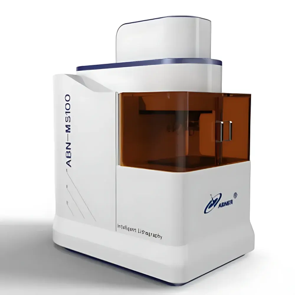
The Abner ABN-MLM-002 Mask Aligner is a precision photolithography instrument engineered for microfabrication in academic research laboratories, MEMS development facilities, and low-volume semiconductor prototyping environments. It operates on the principle of mask-based optical pattern transfer via ultraviolet (UV) radiation—specifically utilizing 365 nm i-line or optional 405 nm UV LED illumination—to induce photochemical reactions in standard positive or negative photoresists. The system supports contact, proximity, and projection exposure modes, enabling resolution down to ≤2 µm under optimal contact conditions. Its robust mechanical architecture integrates a thermally stable optical train, high-rigidity kinematic stage, and vacuum-assisted substrate chucking (optional), ensuring consistent critical dimension (CD) control and overlay fidelity across multi-layer processes. Designed for operational integrity in Class 10,000 cleanroom-equivalent settings, the ABN-MLM-002 meets fundamental requirements for process traceability and reproducibility in GLP-aligned R&D workflows.
Key Features
- Precision alignment subsystem with motorized X/Y/θ motion control and high-magnification CCD imaging—enabling real-time crosshair alignment, image overlay, and sub-2 µm overlay accuracy between mask and substrate;
- Dual-mode exposure capability: selectable contact or proximity configuration with programmable gap control (0–50 µm), facilitating trade-offs between resolution, mask lifetime, and defect tolerance;
- Stabilized UV illumination system featuring either mercury arc lamp (365 nm dominant output) or solid-state UV LED source, both coupled to an integrated homogenizer yielding ≥90% spatial uniformity and ±2% temporal intensity stability over 8-hour continuous operation;
- Modular stage design accommodating 2-inch to 6-inch substrates—including silicon wafers, fused silica, borosilicate glass, quartz, and polyimide-based flexible films—with vacuum chucking (optional) and Z-axis focusing (±5 mm travel, 0.1 µm resolution);
- Full-parameter programmability: exposure dose (via time and intensity), alignment sequence, stage positioning, and interlock logic—all accessible through intuitive touchscreen interface or PC-hosted software;
- Comprehensive safety architecture compliant with IEC 61010-1: includes UV-shielded viewing window (OD4+ at 365 nm), door interlock circuitry, emergency stop activation, and role-based access control for parameter modification;
- Expandable platform supporting factory-installed options including automated mask loader, servo-driven nanometer-precision alignment stage, and Ethernet-enabled remote monitoring with audit trail logging.
Sample Compatibility & Compliance
The ABN-MLM-002 demonstrates broad compatibility with industry-standard photoresists—including AZ series, SU-8, PMMA, and Shipley S18xx formulations—as well as non-silicon substrates such as glass, quartz, sapphire, and polymer foils. Its mechanical and thermal design maintains dimensional stability within ±1 µm over extended thermal cycles (20–25 °C ambient, <60% RH), satisfying baseline environmental criteria for lithographic repeatability. While not certified to ISO 14644-1 Class 100 or SEMI S2/S8, the system is routinely deployed in university cleanrooms and pilot lines operating under ISO Class 7–8 conditions. For regulated applications, optional firmware modules support 21 CFR Part 11-compliant electronic signatures, user activity logging, and parameter change history—enabling alignment with FDA-regulated device prototyping and academic GLP documentation standards.
Software & Data Management
Control is executed via Abner’s proprietary LithoControl™ software suite, available for Windows OS and accessible through USB, RS232, or Ethernet interfaces. The GUI provides dual-mode operation: guided wizard-based workflow for novice users and advanced scriptable mode (TCL/Lua-compatible) for automated recipe chaining. All exposure parameters—including lamp intensity setpoint, dwell time per field, focus offset, and alignment coordinate offsets—are stored in encrypted XML-based project files with version stamping and checksum validation. Audit logs record timestamped operator ID, parameter changes, alarm events, and hardware status snapshots—exportable in CSV or PDF for internal QA review. Integration with LabView and Python APIs enables third-party automation for multi-step process integration (e.g., resist spin-coating → soft bake → alignment → exposure → post-exposure bake).
Applications
- Semiconductor process development: fabrication of test structures, metal interconnects, and passivation windows on Si, GaAs, and SOI wafers;
- MEMS device manufacturing: patterning of piezoresistive elements, comb drives, diaphragms, and release etch windows with layer-to-layer registration ≤2 µm;
- Microfluidic master mold creation: high-fidelity replication of channel networks, mixing chambers, and valve geometries in SU-8 on glass substrates;
- Photonic component prototyping: definition of grating couplers, lenslet arrays, and waveguide cores requiring ≤5 µm feature fidelity;
- 2D materials device engineering: electrode patterning for graphene FETs, TMDC photodetectors, and heterostructure contacts;
- Teaching and training platforms: hands-on instruction in photolithography fundamentals, process window analysis, and defect root-cause investigation.
FAQ
What is the minimum achievable feature size using the ABN-MLM-002?
Under optimized contact-mode conditions with high-resolution photoresist (e.g., AZ 5214E) and calibrated exposure dose, line/space features down to 2 µm are routinely achieved. Sub-µm resolution is not supported due to diffraction-limited optics and mask contact constraints.
Can the system be integrated into a semi-automated fabrication line?
Yes—via optional Ethernet interface and API support, the aligner can synchronize with robotic wafer handlers, track wafer IDs via barcode input, and log exposure metadata to central MES databases.
Is vacuum chucking standard or optional?
Vacuum substrate holding is an optional module; standard configuration uses mechanical clamping with adjustable pressure plates suitable for rigid substrates.
Does the system support alignment to pre-patterned marks on the wafer?
Yes—the CCD alignment system supports fiducial recognition and auto-correlation algorithms for overlay alignment to existing topographical or resist-etched markers, provided sufficient contrast and ≥5 µm mark dimensions.
What maintenance is required for the UV optical path?
Annual inspection and cleaning of quartz condenser lenses and mirror coatings are recommended; mercury lamps require replacement every ~1,000 hours, while UV LEDs offer >10,000-hour lifetimes with minimal intensity drift.


