AcuiTik NS-OEM White Light Interferometric In-Situ Online Thin-Film Thickness Metrology System
| Brand | AcuiTik |
|---|---|
| Origin | Shanghai, China |
| Manufacturer Type | Original Equipment Manufacturer (OEM) |
| Country of Origin | China |
| Model | NS-OEM |
| Wavelength Range | 190–1100 nm |
| Thickness Measurement Range | 1 nm – 1 mm |
| Accuracy | ±2 nm or ±0.2% |
| Static Repeatability | ±0.02 nm |
| Spot Size | 1.5 mm |
| Measurement Speed | <1 s per acquisition |
| Light Source | Tungsten-Halogen Lamp (with optional Deuterium lamp) |
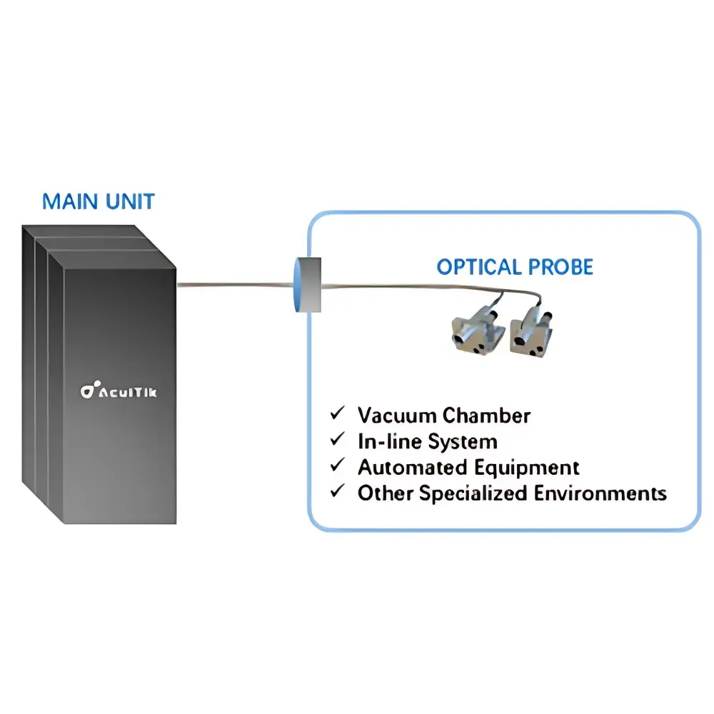
| Probe-to-Host Interface | Fiber Optic (standard length 1.3 m, up to 20 m configurable) |
| Probe Dimensions | Ø19 mm × 86 mm |
| Power Supply | 90–264 VAC, 47–63 Hz |
Overview
The AcuiTik NS-OEM is a compact, fiber-coupled white light interferometric (WLI) thickness metrology system engineered for OEM integration into in-situ, online, and vacuum-compatible environments—including thin-film deposition chambers, roll-to-roll coating lines, semiconductor process tools, and R&D vacuum systems. It operates on the principle of spectral-domain white light interferometry: broadband light (190–1100 nm) is vertically incident onto a multilayer sample; interference fringes generated at each dielectric interface are captured by a high-resolution spectrometer, and layer thicknesses, refractive indices, and reflectance spectra are extracted via proprietary inverse modeling algorithms based on rigorous thin-film optics (Fresnel equations and transfer-matrix formalism). Unlike contact profilometers or ellipsometers, the NS-OEM requires no physical probe contact, eliminating risk of surface damage—making it suitable for soft polymers, fragile organic layers, photoresists, and delicate 2D materials. Its sub-nanometer static repeatability (±0.02 nm) and dual accuracy specification (±2 nm absolute or ±0.2% relative) enable traceable metrology across monolayer graphene (≈0.34 nm) to thick polymer films (>100 µm), supporting both R&D validation and production process control.
Key Features
- Fiber-optic architecture enables physical decoupling of the optical probe from the electronics host—critical for thermal isolation in vacuum chambers or electromagnetic compatibility in plasma-enhanced CVD systems.
- Compact probe (Ø19 mm × 86 mm) with integrated kinematic mounting interface facilitates integration into confined spaces, robotic end-effectors, or multi-axis stages.
- Two spectral configurations available: UV-enhanced (190–1000 nm) for wide-bandgap materials (e.g., AlN, SiC) and VIS-NIR-optimized (350–1100 nm) for silicon photonics and OLED stack characterization.
- Patented PolarX analysis engine implements physics-based forward modeling combined with constrained nonlinear optimization—supporting simultaneous retrieval of thickness, n(λ), k(λ), and interfacial roughness for up to 8-layer stacks without prior knowledge of material dispersion.
- Real-time measurement feedback with <1 s acquisition time enables closed-loop process monitoring during dynamic growth (e.g., ALD pulse-by-pulse verification or sputter rate calibration).
- Full hardware and firmware sovereignty: 100% domestically developed optical design, FPGA-based spectrometer control, and ARM-based embedded host—ensuring supply chain resilience and long-term maintainability.
Sample Compatibility & Compliance
The NS-OEM measures transparent, semi-transparent, and weakly absorbing thin films on rigid (Si, glass, sapphire) or flexible substrates (PET, PI, metal foils). It supports single-layer, bilayer, and complex graded-index or mixed-phase stacks (e.g., ITO/SiO₂/Ag/SiO₂ anti-reflective coatings). Measurement validity is maintained across surface roughness values up to 5 nm RMS (verified per ISO 25178-2), and tilt tolerance is ±1.5°—achievable using the included precision goniometric alignment tool. The system complies with CE marking requirements for electromagnetic compatibility (EN 61326-1) and safety (EN 61010-1). While not pre-certified for FDA 21 CFR Part 11, its PolarX software architecture supports audit trail logging, electronic signature configuration, and role-based access control—enabling qualification under GLP/GMP or ISO 17025 frameworks upon customer-specific validation.
Software & Data Management
PolarX is a Windows-based metrology suite built on Qt and Python (NumPy, SciPy), offering three operational modes: QuickScan (single-point snapshot), MapScan (raster grid acquisition with motorized stage integration), and LiveTrack (continuous temporal monitoring). All raw interferograms and modeled spectra are stored in HDF5 format with embedded metadata (timestamp, environmental sensor readings, user ID, instrument configuration). Batch processing pipelines support automated pass/fail evaluation against user-defined spec limits (e.g., “SiO₂ layer = 95 ± 3 nm”), generating PDF reports compliant with ISO/IEC 17025 clause 7.8. Data export options include CSV, MATLAB .mat, and ASTM E1318-compliant XML schemas. Remote operation is supported via TCP/IP API (RESTful endpoints and WebSocket streaming), enabling integration with MES/SCADA platforms such as Siemens SIMATIC IT or Rockwell FactoryTalk.
Applications
- In-situ monitoring of atomic layer deposition (ALD) and chemical vapor deposition (CVD) processes—tracking nucleation kinetics and growth saturation per cycle.
- Roll-to-roll optical coating QC on flexible displays: real-time thickness uniformity mapping across web widths up to 1.2 m.
- Photovoltaic R&D: quantifying interfacial recombination losses via precise passivation layer (Al₂O₃, SiNₓ) thickness and fixed charge density correlation.
- MEMS fabrication: measuring residual stress-induced curvature in released cantilevers through time-resolved film thickness and substrate bow analysis.
- Biomedical thin films: characterizing hydrogel swelling dynamics and drug-eluting polymer degradation profiles non-destructively.
- Academic nanofabrication: validating layer transfer fidelity in van der Waals heterostructures (e.g., h-BN/MoS₂/graphene stacks).
FAQ
Can the NS-OEM operate inside a UHV chamber (<10⁻⁸ mbar)?
Yes—the optical probe is UHV-compatible (all-metal construction, no outgassing elastomers); fiber feedthroughs use ConFlat flanges with Viton or copper gaskets per customer vacuum specification.
Is calibration traceable to NIST or PTB standards?
Calibration uses SRM 2032 (NIST-traceable SiO₂-on-Si reference wafers) and custom-deposited Ta₂O₅/SiO₂ step-height standards; full uncertainty budget documentation is provided per ISO/IEC 17025 Annex A.
Does PolarX support scripting for automated recipe execution?
Yes—Python API bindings allow full instrument control, data acquisition, and model fitting within Jupyter notebooks or CI/CD pipelines.
What is the minimum measurable thickness for a single SiO₂ layer on silicon?
0.8 nm (limited by signal-to-noise ratio and native oxide interference); typical detection limit is 1 nm with <5% relative uncertainty.
Can the system measure films on curved or textured substrates?
Yes—with optional telecentric objective lens (NA 0.12) and Z-height auto-focus; validated on radius-of-curvature down to 5 mm and Ra ≤ 20 nm machined surfaces.


