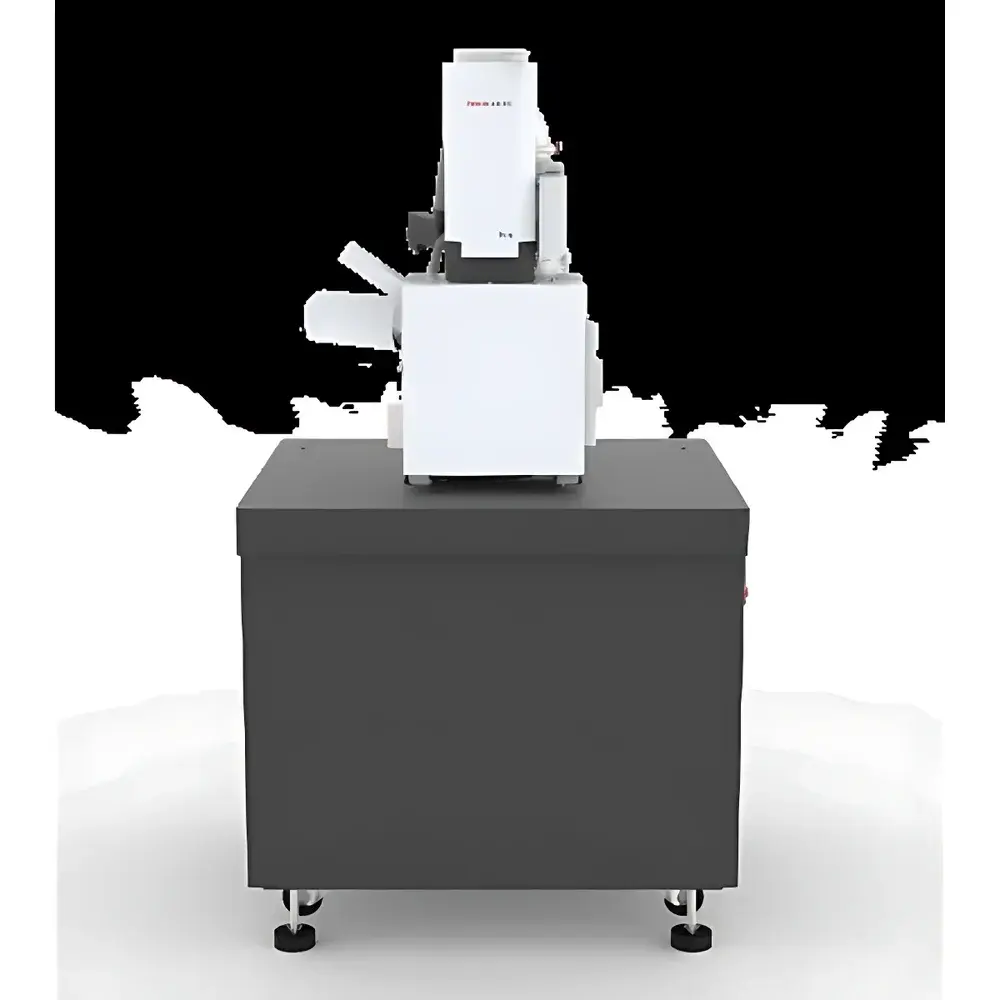
Thermo Fisher Axia ChemiSEM Advanced Real-Time EDS-Integrated Scanning Electron Microscope
| Brand | Thermo Fisher |
|---|---|
| Origin | Shanghai, China |
| Manufacturer Type | Authorized Distributor |
| Origin Category | Domestic (China-Made) |
| Model | Axia ChemiSEM |
| Pricing | Available Upon Request |
Overview
The Thermo Fisher Axia ChemiSEM is an advanced, EDS-integrated scanning electron microscope engineered for seamless morphological imaging and quantitative elemental analysis in a single workflow. Unlike conventional SEMs that require sequential imaging and post-acquisition EDS mapping, the Axia ChemiSEM employs a fully embedded energy-dispersive X-ray spectrometer (EDS) and proprietary real-time signal fusion algorithms to simultaneously acquire backscattered electron (BSE) topographic data and characteristic X-ray spectra. This architecture enables true concurrent imaging and compositional analysis—delivering live, pixel-aligned elemental distribution overlays with quantified weight and atomic percentages directly during beam scanning. Designed for high-throughput laboratory environments, the system operates across vacuum modes—including low-vacuum mode—without mandatory conductive coating, making it suitable for insulating, hydrated, or beam-sensitive specimens while maintaining sub-5 nm resolution at 30 kV.
Key Features
- Real-time EDS integration: Fully embedded silicon drift detector (SDD) EDS system acquires spectral data continuously during imaging; no time lag between morphology and composition acquisition.
- Low-vacuum imaging without sputter coating: Stable operation at pressures up to 130 Pa enables direct observation of non-conductive, porous, or outgassing samples—preserving native surface structure and eliminating coating-induced artifacts.
- Full-color navigation camera: Integrated wide-field optical camera provides real-time, high-fidelity overview of the specimen chamber, enabling rapid sample positioning and stage navigation with centimeter-level spatial awareness.
- Automated alignment and optimization: One-click auto-focus, auto-stigmation, brightness/contrast adjustment, and dynamic beam alignment reduce operator dependency and ensure consistent image quality across magnifications.
- Predetermined hardware configuration: Motorized retractable BSE detector and pre-aligned tungsten or CeB₆ filament minimize manual intervention during setup or maintenance—reducing risk of mechanical damage or misalignment.
Sample Compatibility & Compliance
The Axia ChemiSEM supports a broad range of uncoated and coated specimens, including polymers, ceramics, geological sections, biological tissues (fixed or critical-point dried), metal alloys, and battery electrode materials. Its dual-mode vacuum system (high vacuum ≤1×10⁻³ Pa; low vacuum up to 130 Pa) complies with ASTM E1508–22 for quantitative EDS microanalysis and ISO 16700:2016 for SEM-based particle sizing and morphology assessment. The instrument meets essential electromagnetic compatibility (EMC) and electrical safety requirements per IEC 61000-6-3 and IEC 61010-1, and its software architecture supports audit trails and user access control in accordance with GLP and GMP documentation practices.
Software & Data Management
The Axia ChemiSEM ships with Thermo Scientific™ Maps™ software for automated large-area imaging, mosaic stitching, and region-of-interest (ROI) batch acquisition—enabling unattended overnight data collection. Thermo Scientific™ AutoScript™ provides Python-based scripting capabilities via open API, supporting custom workflows such as automated particle analysis, phase identification, or EDS spectral library matching. All acquired images, spectra, and quantification reports are stored in vendor-neutral formats (e.g., TIFF, .eds, .csv), ensuring long-term data integrity and third-party software interoperability. Data export modules comply with FDA 21 CFR Part 11 requirements for electronic records and signatures when configured with appropriate IT infrastructure.
Applications
- Materials science: Phase distribution mapping in multiphase alloys, inclusion analysis in steels, and interfacial characterization in composite laminates.
- Geosciences: Mineral identification and modal analysis in polished thin sections using ZAF or φ(ρz) quantification models.
- Electronics: Failure analysis of solder joints, contamination detection on PCB surfaces, and cross-sectional analysis of semiconductor packages.
- Life sciences: Cellular ultrastructure imaging of resin-embedded tissues, elemental localization in calcified tissues, and nanoparticle uptake studies.
- Quality control: Rapid verification of coating thickness uniformity, filler dispersion in polymer composites, and defect root-cause analysis in additive manufacturing parts.
FAQ
Does the Axia ChemiSEM require conductive coating for non-metallic samples?
No—low-vacuum imaging mode eliminates the need for sputter coating on most insulating samples, preserving surface fidelity and reducing preparation time.
Can EDS quantification be performed in real time during imaging?
Yes—the integrated EDS detector collects spectra concurrently with BSE imaging, and proprietary algorithms generate live quantitative elemental maps with standardized k-factor corrections.
Is the system compatible with regulatory-compliant data handling protocols?
Yes—when deployed with validated IT controls, the software supports 21 CFR Part 11 compliance, including electronic signatures, audit trails, and role-based access management.
What vacuum modes does the Axia ChemiSEM support?
It operates in both high-vacuum mode (≤1×10⁻³ Pa) for maximum resolution and low-vacuum mode (up to 130 Pa) for charge mitigation on sensitive or non-conductive specimens.
Are automation features limited to basic imaging functions?
No—automation extends to EDS acquisition parameters, map stitching, spectral deconvolution, and report generation via AutoScript™, enabling reproducible, protocol-driven workflows across user skill levels.


