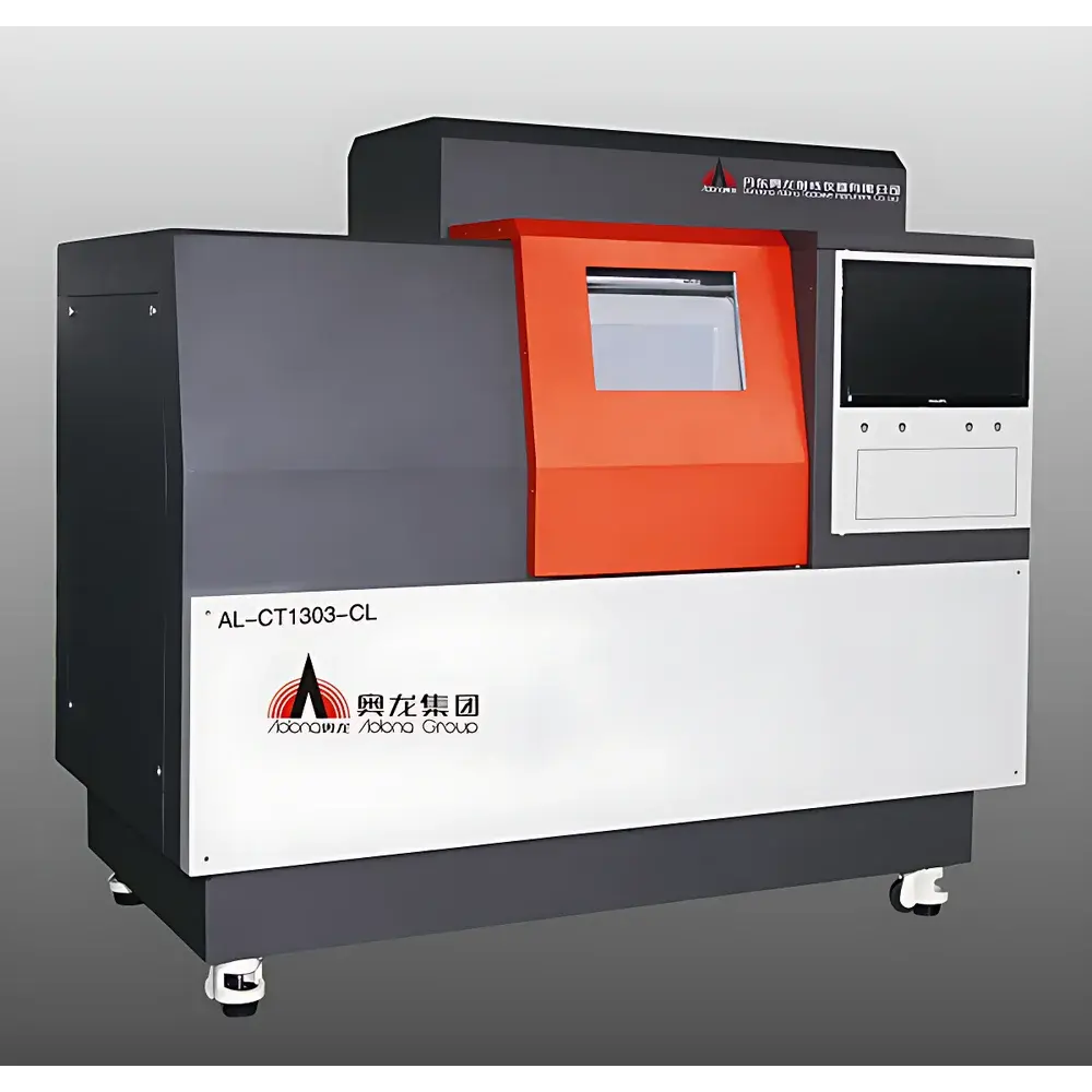
Aolong Planar CT System
| Brand | Aolong |
|---|---|
| Origin | Liaoning, China |
| Manufacturer Type | OEM Manufacturer |
| Regional Classification | Domestic (China) |
| Model | PCB Inspection CT System |
| Quotation | Upon Request |
| X-ray Tube Voltage | 160 kV or 225 kV |
| X-ray Tube Type | Open-type Microfocus Tube |
| Target Geometry | Transmission Target |
| Target Material | Tungsten |
| JIMA Resolution | Up to 0.5 µm |
| Scan Geometry | Cone-beam CT |
| Detector | Digital Flat-panel Detector |
Overview
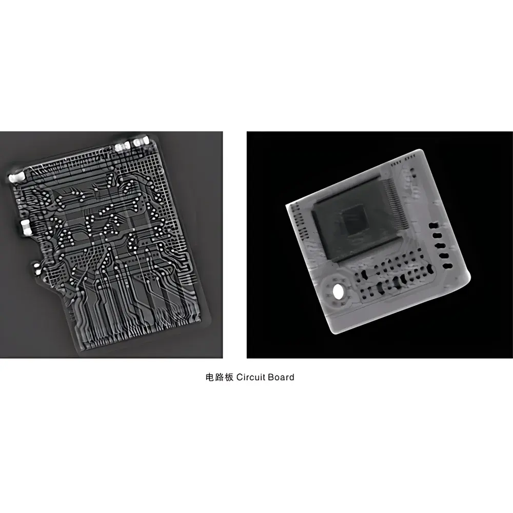
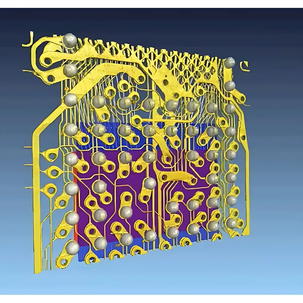
The Aolong Planar CT System is a dedicated industrial micro-computed tomography platform engineered for high-fidelity non-destructive evaluation of planar and layered electronic assemblies. Unlike conventional cone-beam CT systems optimized for isotropic volumetric imaging, this system employs a geometry-optimized acquisition strategy—termed “planar CT”—to maximize spatial resolution and contrast sensitivity within thin, plate-like specimens such as printed circuit boards (PCBs), ball grid arrays (BGAs), surface-mount technology (SMT) assemblies, and stacked semiconductor packages. The system operates on the physical principle of X-ray absorption-based attenuation tomography: a microfocus X-ray source generates a divergent cone beam that penetrates the sample; transmitted photons are captured by a high-dynamic-range digital flat-panel detector; and iterative reconstruction algorithms convert hundreds of angular projections into voxel-resolved 3D volume data. This enables quantitative assessment of internal architecture—including trace continuity, via integrity, solder joint morphology, delamination, voiding, and foreign object debris—without sectioning or destructive cross-sectioning.
Key Features
- Optimized mechanical geometry for planar specimen orientation, minimizing parallax error and maximizing effective resolution in the XY plane and Z-depth slicing accuracy.
- Open-type microfocus X-ray tube with selectable operating voltages (160 kV / 225 kV), enabling flexible penetration control for multi-material assemblies—from FR-4 substrates to copper traces, solder alloys, and ceramic passives.
- Transmission-mode tungsten target delivering stable, high-brightness focal spots down to sub-micron dimensions, essential for resolving fine features such as 5-µm traces or 25-µm solder balls.
- JIMA-certified spatial resolution up to 0.5 µm under optimal magnification and exposure conditions—validated per ISO 16508-2 and ASTM E2737 standards for microfocus CT performance assessment.
- Cone-beam scanning architecture with precise rotational and translational stage control, supporting both full 360° acquisition and partial-angle helical or step-and-shoot protocols tailored to PCB-specific workflows.
- Integrated thermal management and vibration-damping base structure ensuring long-term stability during multi-hour acquisitions required for high-SNR reconstructions.
Sample Compatibility & Compliance
The Aolong Planar CT System accommodates specimens up to 300 mm × 300 mm in footprint and 50 mm in thickness, with standardized fixtures for rigid PCBs, flex-rigid hybrids, and encapsulated modules. It supports non-destructive inspection of multilayer PCBs (up to 32 layers), flip-chip packages, wafer-level CSPs, and MEMS/MOEMS devices containing silicon, glass, and polymer components. All system firmware and acquisition software comply with ISO/IEC 17025 requirements for testing laboratories, and raw projection data storage adheres to DICOM-CT Part 10 conventions. Reconstructed volumes are exportable in standard formats (e.g., TIFF stack, NRRD, STL) compatible with third-party metrology and CAD reverse-engineering tools. The system design meets CE electromagnetic compatibility (EMC) directives and IEC 61000-6-3 emission limits. Radiation shielding conforms to national GBZ 130–2020 safety standards for industrial X-ray equipment.
Software & Data Management
The proprietary reconstruction suite includes GPU-accelerated FDK and iterative SART algorithms, with optional regularization for low-dose or limited-angle scenarios. Volume rendering, slice navigation, and region-of-interest (ROI) segmentation are performed in real time using hardware-accelerated OpenGL pipelines. Quantitative analysis modules support automated void detection, porosity mapping, solder joint classification (per IPC-A-610 Class 2/3 criteria), and trace width/thickness metrology traceable to NIST-calibrated phantoms. Audit trails record all user actions, parameter changes, and reconstruction settings in compliance with GLP and FDA 21 CFR Part 11 requirements when configured with electronic signature modules. Data archiving follows hierarchical storage management (HSM) protocols, with metadata embedded per MIAME/MIACA guidelines for long-term reproducibility.
Applications
- Failure analysis of open/short circuits, tombstoning, head-in-pillow defects, and intermetallic growth in BGA/CSP solder joints.
- Verification of via-in-pad plating quality, buried via alignment, and microvia reliability in HDI PCBs.
- Reverse engineering of legacy PCBs via automatic centerline extraction and netlist generation for CAD re-synthesis (e.g., Gerber/ODB++ export).
- Process validation for conformal coating uniformity, underfill capillary flow, and adhesive bond line integrity in module-level assembly.
- Qualification of MEMS packaging hermeticity through sealed cavity gas volume quantification and crack path tracing.
- Support for automotive AEC-Q200 qualification testing, aerospace AS9100 process audits, and medical electronics ISO 13485 design verification.
FAQ
What distinguishes planar CT from conventional micro-CT?
Planar CT uses a fixed geometry optimized for flat samples—minimizing geometric unsharpness and enhancing Z-resolution perpendicular to the board plane—whereas standard micro-CT prioritizes isotropic voxel fidelity across arbitrary orientations.
Can the system perform quantitative dimensional metrology?
Yes—when calibrated with certified step-height and sphere phantoms, it achieves measurement uncertainties ≤ ±1.5 µm (k=2) for feature sizes >5 µm, compliant with VDI/VDE 2630-1.1.
Is CAD model reconstruction supported out of the box?
The system includes automated trace segmentation and layer registration tools; final CAD export (e.g., STEP, IDF) requires integration with licensed ECAD platforms such as Cadence Allegro or Zuken CR-8000.
Does the system support automated defect classification?
AI-assisted classification models (e.g., for solder voids, cracks, or bridging) can be deployed via API integration with trained TensorFlow/PyTorch inference engines—custom training datasets are customer-provided.
What radiation safety certifications does the system hold?
It carries full type approval per China’s National Standard GBZ 130–2020 and includes interlocked shielding doors, dose-rate monitoring sensors, and emergency stop circuits meeting IEC 61511 SIL-2 requirements.
Related Products


