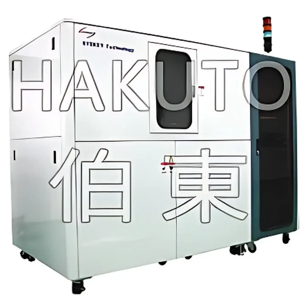
Syskey Thermal Atomic Layer Deposition System
| Brand | Syskey |
|---|---|
| Origin | Taiwan |
| Model | Thermal ALD |
| Substrate Size | Customizable, up to 300 mm wafer |
| Process Temperature | Up to 400 °C (substrate heater) |
| Uniformity | ±1% |
| Precursor Channels | Up to 6, each independently heated to 200 °C |
| Pulse Valve Response Time | 10 ms |
| Chamber Material | Aluminum or stainless steel |
| Cooling | Integrated water-cooling system |
Overview
The Syskey Thermal Atomic Layer Deposition (ALD) System is a high-precision, batch-capable thin-film growth platform engineered for research and pilot-scale semiconductor fabrication. Operating on the fundamental principle of self-limiting surface reactions, this thermal ALD system sequentially introduces gaseous precursors into a reaction chamber under controlled vacuum conditions. Each precursor chemisorbs onto the substrate surface in a saturated monolayer, followed by a purge step to remove excess molecules and byproducts—ensuring atomic-level thickness control and exceptional conformality. Unlike plasma-enhanced ALD (PE-ALD), thermal ALD relies solely on thermally activated surface chemistry, making it ideal for applications requiring minimal ion bombardment, low defect density, and high film stoichiometry—particularly in gate dielectrics, passivation layers, and encapsulation films for OLEDs, photovoltaics, and MEMS.
Key Features
- Thermally stable substrate heating up to 400 °C with <±0.5 °C setpoint accuracy and spatial uniformity across full 300 mm wafers
- Independent temperature control for up to six precursor delivery lines, each capable of heating to 200 °C to ensure consistent vapor pressure and prevent condensation
- Ultra-fast pneumatic pulse valves with 10 ms actuation time for precise temporal control of precursor exposure—critical for reproducible cycle definition and minimal cross-contamination
- Modular chamber architecture available in aluminum (anodized) or electropolished stainless steel variants, optimized for ultra-high vacuum (UHV)-compatible base pressures (<1×10⁻⁷ mbar)
- Integrated water-cooling jacket for rapid thermal stabilization and chamber wall temperature management during extended process runs
- Compact footprint design enabling seamless integration with load-lock modules, robotic transfer arms, and inert-atmosphere gloveboxes (N2/Ar <1 ppm O2/H2O)
Sample Compatibility & Compliance
The system supports customizable substrate carriers accommodating wafers from 100 mm to 300 mm diameter, as well as non-standard geometries including diced dies, microfluidic chips, and nanostructured templates. Film uniformity is validated per SEMI F47 and ISO/IEC 17025–accredited metrology protocols, demonstrating ≤±1% thickness variation across full-wafer maps (measured via ellipsometry and XRF). Chamber materials and seals comply with ASTM F2298 (high-purity semiconductor processing components) and meet outgassing requirements specified in NASA SP-R-1 (Rev. B) for low-volatility environments. Optional residual gas analyzers (RGAs) and quadrupole mass spectrometers support real-time process monitoring aligned with ISO 9001:2015 quality management frameworks.
Software & Data Management
Control is executed via a deterministic real-time operating system (RTOS) with deterministic I/O latency (<100 µs). The GUI-based software suite provides full recipe scripting—including multi-step sequences with conditional logic, interlock validation, and hardware fault logging. All process parameters (temperature ramps, pulse durations, purge times, pressure profiles) are timestamped and stored in encrypted SQLite databases compliant with FDA 21 CFR Part 11 Annex 11 requirements for electronic records and signatures. Audit trails record user login/logout events, parameter modifications, and alarm acknowledgments—supporting GLP/GMP audit readiness. Export formats include CSV, HDF5, and XML for traceable integration with LIMS and MES platforms.
Applications
- High-κ gate oxides (Al2O3, HfO2, Ta2O5) for advanced CMOS nodes
- Passivation layers (Al2O3, SiO2) in PERC and TOPCon solar cells
- Encapsulation barriers (AlN, SiNx) for flexible OLED displays and micro-LED arrays
- Functional coatings on high-aspect-ratio MEMS structures (e.g., gyroscope proof masses, RF resonators)
- Atomic-scale seed layers for selective electroplating in advanced packaging (2.5D/3D IC interconnects)
- Functionalized nanoporous membranes for sensing and filtration applications
FAQ
What vacuum level does the system achieve before precursor introduction?
Base pressure is typically <1×10⁻⁷ mbar using turbomolecular pumping backed by dry scroll pumps—verified with calibrated Bayard-Alpert gauges.
Can the system be upgraded to support plasma-assisted ALD (PE-ALD)?
Yes—the chamber flange configuration and electrical feedthroughs allow retrofitted RF or microwave plasma sources compatible with industry-standard 13.56 MHz or 2.45 GHz generators.
Is remote diagnostics and predictive maintenance supported?
The system includes OPC UA server functionality for secure third-party SCADA integration, enabling real-time health monitoring of heater elements, valve actuators, and vacuum gauges.
Are process recipes transferable between different Syskey ALD tools?
Yes—recipe files are platform-agnostic and version-controlled; calibration offsets (e.g., temperature sensor drift compensation) are stored separately to ensure cross-tool reproducibility.
Does the system support in-situ ellipsometry or QCM monitoring?
Standard configurations include CF-100 flanges for integration of commercial spectroscopic ellipsometers or quartz crystal microbalances—electrical and mechanical interfaces are pre-engineered for plug-and-play installation.


