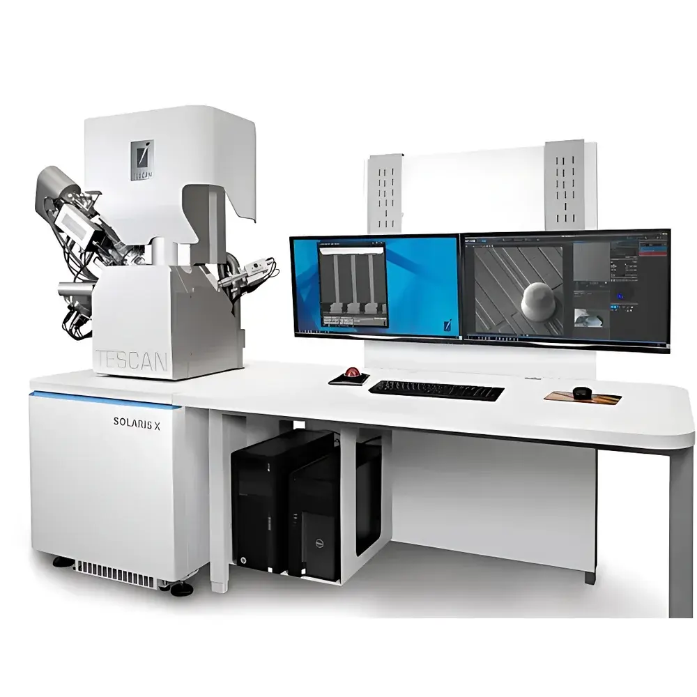
TESCAN SOLARIS X Xenon Plasma Dual-Beam FIB-SEM System
| Brand | TESCAN |
|---|---|
| Origin | Czech Republic |
| Manufacturer Type | Original Equipment Manufacturer (OEM) |
| Category | Imported Instrument |
| Model | TESCAN SOLARIS X |
| Price Range | USD 1.3M – 1.9M |
Overview
The TESCAN SOLARIS X is a high-performance xenon (Xe) plasma dual-beam focused ion beam–scanning electron microscope (FIB-SEM) system engineered for nanoscale characterization and large-volume 3D microanalysis in advanced materials science, semiconductor failure analysis, and life sciences. Unlike conventional gallium (Ga⁺) FIB systems, the SOLARIS X leverages a high-current Xe plasma ion source—offering significantly reduced ion implantation depth, minimal lattice amorphization, and no reactive metal contamination—making it uniquely suited for preparing artifact-free transmission electron microscopy (TEM) lamellae, cross-sectioning packaged ICs, and performing quantitative 3D structural and compositional analysis. At its core, the system integrates two purpose-built, co-aligned mirror columns: the Triglav™ ultra-high-resolution (UHR) SEM column featuring a Schottky field-emission electron gun and a novel TriLens™ three-stage electromagnetic lens system, and the iFIB+™ Xe plasma FIB column delivering up to 2 µA ion current while maintaining sub-10 nm probe stability at 30 kV. This architecture enables simultaneous high-fidelity imaging, precision milling, and in situ analytical data acquisition—including energy-dispersive X-ray spectroscopy (EDS), electron backscatter diffraction (EBSD), and time-of-flight secondary ion mass spectrometry (TOF-SIMS)—within a single vacuum chamber.
Key Features
- Triglav™ UHR SEM column with TriLens™ electromagnetic optics and integrated TriSE™/TriBE™ multi-angle signal detection for enhanced surface sensitivity and contrast on insulating or beam-sensitive specimens.
- iFIB+™ Xe plasma FIB column offering industry-leading field-of-view (>1 mm at 30 kV) and high sputter rates—enabling rapid cross-sectioning of MEMS devices, OLED displays, and full-die IC packages.
- OptiGIS™ gas injection system configurable with up to six independent nozzles or a 5-nozzle inline multi-GIS unit, supporting validated chemistries for selective etching, deposition, and passivation in packaging FA workflows.
- Essence™ software platform with application-specific wizards, semi-automated beam alignment routines, DrawBeam™ vector scanning engine, and collision modeling for robust workflow reproducibility and GLP-compliant audit trails.
- Piezoelectric-driven aperture selector with 30 discrete apertures—ensuring long-term beam stability, minimized maintenance intervals, and rapid switching between milling, polishing, and nanofabrication modes.
- In-chamber axial BSE detector with energy filtering capability to isolate low-energy backscattered electrons—improving topographic contrast and surface-layer sensitivity without charge compensation.
Sample Compatibility & Compliance
The SOLARIS X accommodates samples up to 8-inch (200 mm) wafers and supports fully automated stage navigation across large-area substrates—critical for wafer-level failure analysis and process control metrology. Its wide working distance (up to 40 mm) and 60° objective lens geometry ensure uniform resolution and signal collection over complex topographies, including stacked dies, heterogeneous composites, and biological tissue blocks embedded in resin. The system complies with ISO 14644-1 Class 5 cleanroom requirements for vacuum chamber construction and meets electromagnetic compatibility standards per IEC 61326-1. All software modules support 21 CFR Part 11-compliant electronic signatures, audit logging, and user-access tiering—facilitating GMP/GLP-regulated environments in semiconductor manufacturing and medical device R&D.
Software & Data Management
Essence™ provides a modular, role-based interface with customizable dashboards, scriptable automation via Python API, and native integration with third-party reconstruction tools (e.g., Avizo, Dragonfly). Raw FIB-SEM tomography datasets—including sequential SE/BSE images, EDS hypermaps, and EBSD orientation maps—are stored in vendor-neutral HDF5 format with embedded metadata (acquisition parameters, stage coordinates, beam conditions). The platform supports real-time correlation of ion beam milling progress with electron image feedback, enabling adaptive slice-and-view protocols. For regulatory traceability, every session generates timestamped, digitally signed log files compliant with ASTM E2917 and ISO/IEC 17025 documentation requirements.
Applications
- 3D microstructural analysis of interconnects, TSVs, solder joints, and grain boundaries in advanced nodes (≤5 nm logic, 1β DRAM).
- Non-destructive delayering of fan-out wafer-level packages (FOWLP) and chip-on-film (COF) assemblies using Xe⁺-assisted gas-enhanced etching.
- High-fidelity TEM lamella preparation from beam-sensitive battery cathodes, 2D materials (e.g., graphene/SiAlON heterostructures), and frozen-hydrated cryo-specimens.
- Nanoscale circuit edit and maskless lithography via DrawBeam™ vector patterning—supporting rapid prototyping of plasmonic metasurfaces and quantum dot arrays.
- Correlative TOF-SIMS/EDS/EBSD mapping of dopant segregation, interfacial oxidation, and phase evolution in thermally cycled power electronics.
FAQ
How does Xe plasma FIB compare to Ga⁺ FIB in terms of sample damage?
Xe⁺ ions exhibit ~5× shallower implantation depth and ~3× smaller interaction volume than Ga⁺ at equivalent energies—reducing subsurface amorphization and eliminating Ga-related spectral interferences (e.g., Ga L-lines overlapping Ce M, Ge L, or Ga K peaks in EDS/TOF-SIMS).
Can the SOLARIS X perform automated serial sectioning for 3D EBSD?
Yes—the system supports synchronized FIB milling and EBSD pattern acquisition at each slice, with post-processing pipelines for crystallographic reconstruction and grain boundary network analysis.
Is wafer-scale navigation supported for 8-inch substrates?
Yes—motorized 5-axis stage with laser-interferometric position feedback enables sub-micron repeatability across full 200 mm wafers, including edge-to-edge SEM/FIB inspection without manual repositioning.
What level of software validation is available for regulated industries?
Essence™ includes IQ/OQ documentation templates, 21 CFR Part 11 compliance modules, and configurable electronic signature workflows aligned with FDA and EU Annex 11 expectations.
Does the system support in situ heating or cooling stages?
Yes—optional compatible holders include MEMS-based heating stages (up to 1000 °C), cryo-transfer systems (−180 °C), and electrochemical liquid cells—all integrated with real-time signal synchronization in Essence™.


