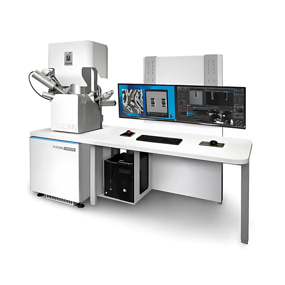
TESCAN AMBER Ga⁺ Focused Ion Beam-Scanning Electron Microscope (FIB-SEM)
| Brand | TESCAN |
|---|---|
| Origin | Czech Republic |
| Manufacturer Type | Original Equipment Manufacturer (OEM) |
| Origin Category | Imported Instrument |
| Model | TESCAN AMBER |
| Price Range | USD 920,000 – 1,315,000 |
Overview
The TESCAN AMBER is the fourth-generation focused ion beam–scanning electron microscope (FIB-SEM) platform developed by TESCAN, a leading European manufacturer of advanced electron microscopy systems. Engineered for nanoscale characterization, in situ manipulation, and precision sample preparation, the AMBER integrates a high-performance Ga⁺ liquid metal ion source (LMIS) FIB column with a field-emission SEM column—both co-aligned within a single, ultra-stable vacuum chamber. Its core architecture is built upon two proprietary innovations: the BrightBeam™ electron optical column, which eliminates stray magnetic fields via a fully electrostatic–electromagnetic hybrid objective lens, and the Orage™ Ga⁺ FIB column, delivering ion beam currents up to 100 nA and energy tunability down to 500 eV. This dual-column design enables simultaneous or sequential high-resolution imaging, compositional analysis, cross-sectional milling, TEM lamella preparation, and nanofabrication—all under real-time visual feedback. The system is designed for rigorous R&D environments in semiconductor metrology, materials science, geoscience, life sciences (including cryo-FIB workflows), and battery research, where reproducibility, spatial fidelity, and analytical versatility are non-negotiable.
Key Features
- BrightBeam™ electron column featuring an aberration-optimized, field-free objective lens—enabling high-resolution (<1.0 nm at 1 kV), low-voltage imaging of magnetic, beam-sensitive, and non-conductive samples without signal distortion from residual magnetic fields.
- Orage™ Ga⁺ FIB column with auto-alignment functionality, offering continuous energy tuning (0.5–30 keV), beam current up to 100 nA, and SmartMill™ high-speed milling mode—doubling material removal rates while preserving subsurface integrity.
- Integrated OptiGIS™ single-nozzle gas injection system with quick-change gas cylinder interface—supporting deposition (W, Pt, C, SiOx) and enhanced etching (XeF2, H2O) without compromising chamber real estate or vacuum stability.
- Four next-generation detectors: In-lens Axial Detector, MultiDetector™ (with variable bias and angular selectivity), STEM-in-SEM detector, and optional backscattered electron (BSE) detector—enabling nine distinct contrast modalities and quantitative signal separation for topographic, compositional, and crystallographic interpretation.
- Large-volume specimen chamber (Ø 240 mm × H 260 mm) with >20 standardized ports—including provisions for in situ heating, cooling, mechanical testing, EBSD, EDS, and direct integration with TOF-SIMS and confocal Raman spectrometers.
- Essence™ 3.0 software platform with guided workflow automation, real-time 3D collision-avoidance simulation, customizable user profiles, and full compliance with FDA 21 CFR Part 11 audit trail requirements for regulated laboratories.
Sample Compatibility & Compliance
The TESCAN AMBER accommodates specimens up to 150 mm in diameter and 50 mm in height, including wafers, polished cross-sections, biological cryo-lamellae, geological thin sections, and packaged microelectronic devices. Its low-kV SEM capability ensures charge-free imaging of insulators without sputter coating; its sub-1 keV FIB mode enables damage-free surface cleaning and ultrathin TEM lamella final polishing. The system meets ISO 14644-1 Class 5 cleanroom compatibility standards for vacuum chamber construction and adheres to IEC 61000-6-3/6-4 electromagnetic compatibility specifications. All software operations—including method saving, parameter logging, and image annotation—support ALCOA+ principles (Attributable, Legible, Contemporaneous, Original, Accurate, Complete, Consistent, Enduring, Available) required under GLP and GMP frameworks.
Software & Data Management
Essence™ 3.0 provides a role-based, modular interface with drag-and-drop workflow builders for routine tasks such as automated lamella lift-out, serial sectioning, and particle analysis. Raw data—including SEM/FIB images, stage coordinates, beam parameters, and detector signals—are stored in vendor-neutral HDF5 format with embedded metadata (EXIF-compliant). Integrated scripting (Python API) supports custom automation, batch processing, and integration with third-party analysis tools (e.g., DigitalMicrograph, MATLAB, Avizo). Audit trails record every user action with timestamp, IP address, and electronic signature—fully traceable for regulatory review. Optional cloud synchronization enables secure remote monitoring and collaborative annotation across distributed research teams.
Applications
- TEM sample preparation: Site-specific, low-damage lamella extraction from IC devices, solid-state batteries, and heterogeneous catalysts.
- In situ nanomechanical testing: Real-time observation of crack propagation, phase transformation, and grain boundary sliding during nanoindentation or tensile straining.
- 3D correlative microscopy: Registration of FIB-SEM tomography with synchrotron X-ray CT or cryo-ET datasets.
- Failure analysis: Cross-sectional inspection of solder joints, via structures, and gate oxides in advanced nodes (≤3 nm).
- Geological petrography: Quantitative pore-throat network reconstruction in shale reservoir rocks and carbonate diagenetic textures.
- Biological ultrastructure: Cryo-FIB milling of vitrified cells followed by STEM tomography and correlative fluorescence mapping.
FAQ
What is the minimum achievable FIB landing energy on the TESCAN AMBER?
The Orage™ Ga⁺ column supports continuous energy tuning from 500 eV to 30 keV, enabling ultra-low-energy surface modification and minimal subsurface damage.
Does the system support automated TEM lamella preparation?
Yes—Essence™ includes preconfigured, validated workflows for lift-out, thinning, and polishing, compliant with ASTM E2979-20 standards for electron microscopy sample preparation.
Can the AMBER be integrated with time-of-flight secondary ion mass spectrometry (TOF-SIMS)?
Yes—TESCAN offers factory-integrated TOF-SIMS coupling via a differential pumping interface and synchronized stage control, enabling simultaneous FIB milling and molecular surface mapping.
Is the BrightBeam™ column compatible with magnetic materials?
Absolutely—the field-free design eliminates Lorentz force deflection, permitting high-resolution imaging and EBSD analysis of ferromagnetic alloys, permanent magnets, and spintronic heterostructures without demagnetization.
What vacuum level is maintained in the specimen chamber during operation?
The chamber achieves ≤2 × 10⁻⁷ mbar base pressure using a combination of turbomolecular and ion pumps, with dynamic pressure stabilization during GIS gas injection to ensure consistent beam performance.


