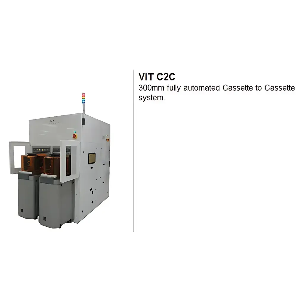
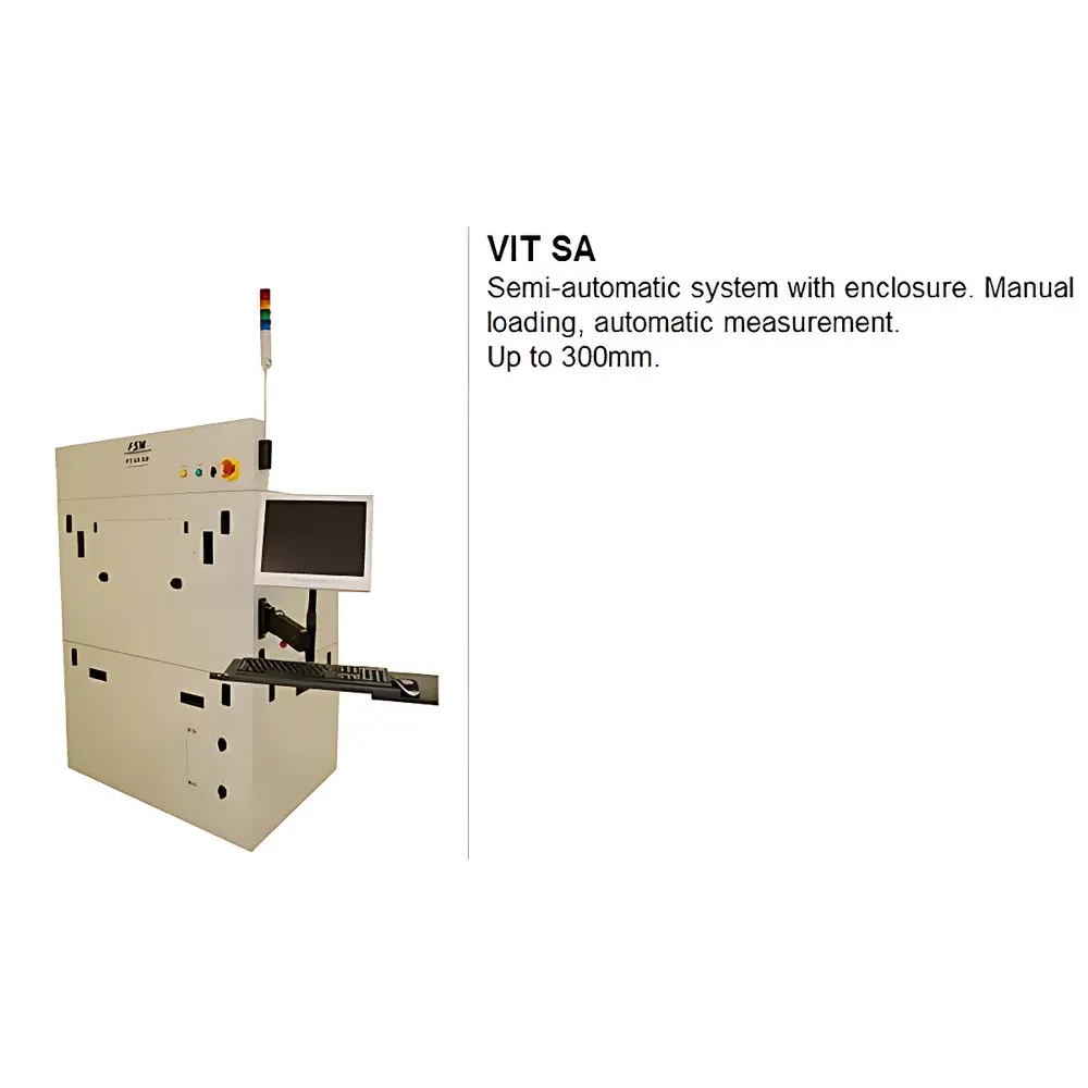
FSM VIT Series Silicon Wafer Surface Topography Metrology System
| Brand | FSM |
|---|---|
| Origin | USA |
| Manufacturer Type | Authorized Distributor |
| Product Origin | Imported |
| Model | VIT |
| Pricing | Available Upon Request |
Overview
The FSM VIT Series is a non-contact, high-resolution optical metrology platform engineered for 3D integrated circuit (3D-IC) process control and advanced wafer-level characterization. Leveraging Virtual Interface Technology (VIT), the system enables rapid, quantitative 3D surface topography mapping of silicon wafers without physical probe contact or vacuum requirements. Its core measurement principle combines multi-angle interferometric profilometry with advanced phase-shifting algorithms to resolve sub-nanometer vertical height variations and micron-scale lateral features across full 200 mm and 300 mm wafers. Designed specifically for front-end-of-line (FEOL) and back-end-of-line (BEOL) process development, the VIT Series supports critical dimensional metrology tasks including through-silicon via (TSV) profile analysis, copper pillar height quantification, bump geometry assessment, and edge-trim contour characterization — all traceable to NIST-calibrated standards and compatible with industry-standard SEMI E142 and ASTM F3019 workflows.
Key Features
- Virtual Interface Technology (VIT): Eliminates mechanical scanning artifacts by optically synthesizing virtual reference surfaces for robust height reconstruction across varying reflectivity and step heights.
- Full-wafer TSV metrology: Measures depth, bottom critical dimension (CD), sidewall angle (SWA), tilt, and residue presence in single-acquisition mode with ≤5 nm vertical repeatability (3σ).
- Copper nail and RST (residue after CMP) detection: Differentiates conductive vs. dielectric residues using spectral reflectance contrast analysis at multiple wavelengths (405–660 nm).
- Bump and Cu pillar height mapping: Quantifies height uniformity, coplanarity, and solder volume across arrays up to 100×100 elements per field, supporting JEDEC JESD22-B111 compliance verification.
- Edge trim profile analysis: Captures bevel and edge exclusion zone geometry within ±0.1 mm radial tolerance, aligned with SEMI MF1530 specifications for edge die yield modeling.
- Thin wafer compatibility: Stable operation on wafers down to 50 µm thickness without carrier support, enabled by adaptive focus tracking and low-coherence illumination.
Sample Compatibility & Compliance
The VIT Series accommodates bare silicon, SiO₂/SiNₓ films, low-k dielectrics, electroplated Cu, Ni, and SnAg alloys, as well as temporary bonding layers used in hybrid bonding stacks. All measurement modes comply with ISO/IEC 17025-accredited calibration protocols and support GLP/GMP audit readiness via configurable user access levels, electronic signatures, and full audit trail logging (21 CFR Part 11 compliant when deployed with FSM’s SecureLog™ software module). Data outputs conform to SEMI E139 (wafer map XML) and ASTM E2917 (metrology uncertainty reporting) standards.
Software & Data Management
Controlled via FSM’s MetroSuite™ v5.2 platform, the system provides scriptable measurement recipes, automated defect-flagging logic, and cross-tool SPC integration through SECS/GEM interfaces. Raw height maps are stored in HDF5 format with embedded metadata (tool ID, recipe version, operator ID, timestamp, environmental conditions). Batch analysis supports wafer-to-wafer and lot-to-lot trend reporting with statistical summaries (mean, std dev, min/max, Cp/Cpk) exportable to JMP, Minitab, or factory MES systems. Optional cloud-sync capability enables remote review and cross-site correlation without compromising data sovereignty.
Applications
- TSV etch and fill process monitoring: Depth uniformity, CD taper, and bottom rounding evaluation for 5–50 µm diameter vias.
- Post-CMP residue classification: Discrimination between Cu oxide, silica slurry remnants, and organic polymer residues based on spectral signature clustering.
- Hybrid bonding alignment stack metrology: Quantitative assessment of Cu pillar height distribution, planarity deviation (<±0.3 µm), and interfacial gap variation prior to thermocompression.
- Film stress-induced wafer bow measurement: Integration with FSM’s Film Stress Module enables curvature-derived stress calculation per ASTM F390, supporting FEOL thin-film qualification.
- Edge die yield optimization: Correlation of edge-trim geometry with electrical test fallout to refine dicing street design rules.
FAQ
Does the VIT Series require vacuum or sample coating?
No. It operates under ambient atmospheric conditions and requires no sputter coating, making it suitable for in-line process monitoring and post-fabrication inspection.
Can it measure transparent or highly reflective films?
Yes. Multi-wavelength illumination and adaptive gain control enable stable profiling on SiO₂, SiNₓ, and polished Cu surfaces without saturation or fringe ambiguity.
Is tool-to-tool matching supported?
Yes. FSM provides inter-tool correlation packages certified to ≤1.5 nm height bias (k=2) across VIT installations, validated per ASTM E2523.
What wafer handling options are available?
Standard load ports support FOUPs (SEMI E47.1) and open cassettes; optional robotic integration complies with SEMI E84 and E157 specifications.
How is calibration maintained?
Traceable NIST-certified step-height standards are used for daily verification; annual recalibration is performed by FSM-certified field service engineers following ISO 17025 procedures.


