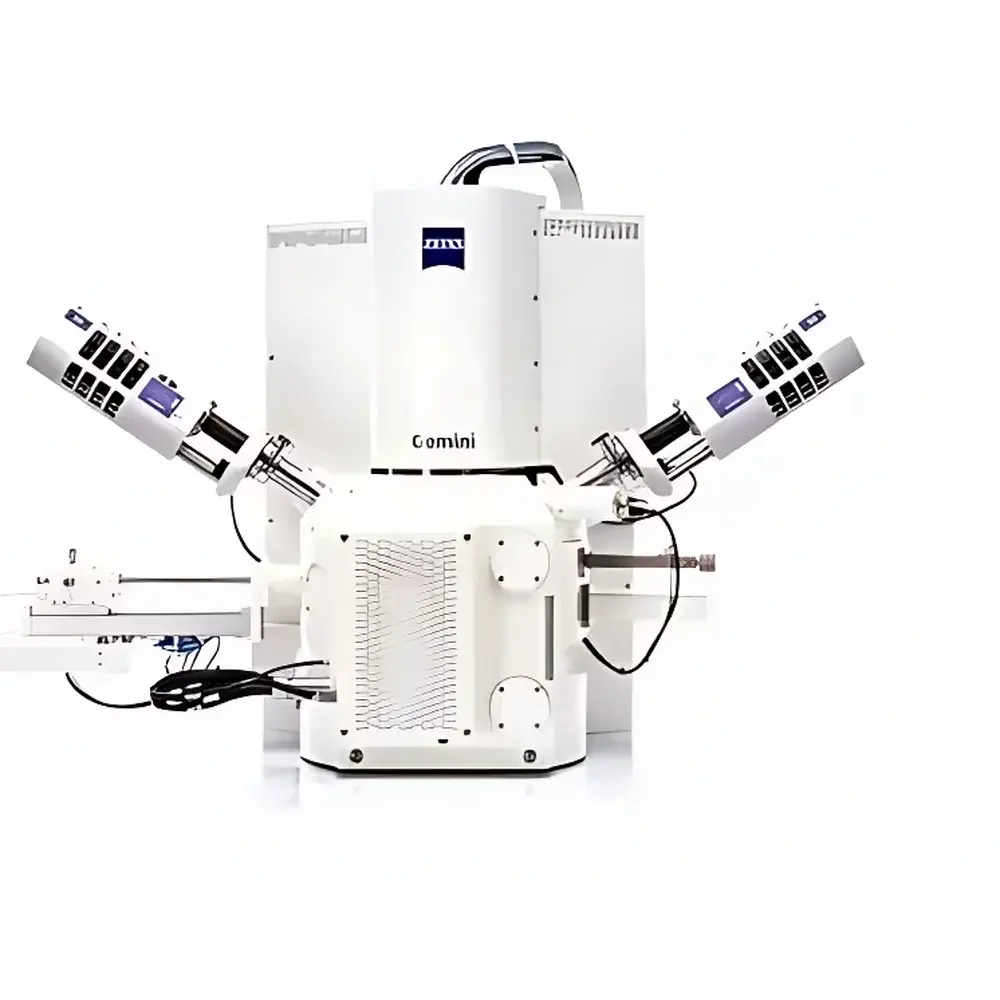
ZEISS SIGMA Field Emission Scanning Electron Microscope
| Brand | ZEISS |
|---|---|
| Origin | Germany |
| Manufacturer Type | Authorized Distributor |
| Origin Category | Imported |
| Model Series | SIGMA |
| Instrument Type | Desktop SEM |
| Electron Gun Type | Cold Field Emission |
| Microscope Class | High-Resolution Field Emission SEM |
| Secondary Electron (SE) Image Resolution | 1.0 nm @ 1 kV, 0.8 nm @ 3 kV |
| Maximum Magnification | 1,000,000× |
| Accelerating Voltage Range | 0.02–30 kV |
| Backscattered Electron (BSE) Image Resolution | 3.0 nm @ 30 kV |
| Working Distance for Analysis | 8.5 mm |
| Tilt Angle for EDS Collection | 35° |
| Variable Pressure Mode | Yes (C2D & VP-SE Detectors) |
| In-Lens SE/BSE Dual Detection | Yes |
| STEM-in-SEM Capability | Yes (aSTEM Detector Optional) |
| EDS Integration | SmartEDX (Si(Li)/SDD, Nitride Window Optimized for Light Elements) |
| RISE Integration | Yes (Fully Integrated Confocal Raman Imaging) |
Overview
The ZEISS SIGMA Field Emission Scanning Electron Microscope is an advanced desktop-class analytical platform engineered for high-resolution imaging, compositional analysis, and correlative multimodal characterization in academic, industrial, and quality control laboratories. Built upon the proven Gemini electron optical column—ZEISS’s proprietary dual-lens design that synergistically optimizes electrostatic and magnetic fields—the SIGMA delivers exceptional beam stability, sub-nanometer probe convergence, and minimal sample charging or drift, even on insulating or beam-sensitive specimens. Its cold field emission (CFE) electron source ensures long-term brightness stability and ultra-fine probe formation across the full accelerating voltage range (20 V to 30 kV), enabling both low-voltage surface-sensitive imaging and high-penetration elemental excitation. The system operates in three distinct vacuum regimes—high vacuum (HV), low vacuum (LV), and variable pressure (VP)—to accommodate diverse sample types without mandatory conductive coating.
Key Features
- Gemini II electron optics with in-lens detection architecture for simultaneous high-efficiency secondary electron (SE) and backscattered electron (BSE) signal collection
- Four-step guided workflow (Navigate → Set Conditions → Optimize Region → Acquire & Visualize) for rapid, repeatable operation in multi-user environments
- Dual-mode detection: ETSE (Everhart-Thornley SE) and in-lens SE detectors for topographic contrast; C2D and VP-SE detectors for enhanced signal yield (up to 85% contrast retention) in low-vacuum mode
- Optimized analytical geometry: 8.5 mm working distance and 35° take-off angle maximize X-ray collection efficiency for energy-dispersive spectroscopy (EDS)
- aSTEM detector integration for scanning transmission electron microscopy (STEM)-in-SEM imaging at nanoscale resolution
- SmartEDX EDS system with ultrathin silicon nitride window and SDD detector, enabling quantitative light-element detection (Be–U) and spatially resolved mapping
- RISE (Raman Imaging and Scanning Electron Microscopy) module for fully integrated confocal Raman spectroscopy, delivering molecular fingerprinting co-registered with SEM morphology and EDS chemistry
Sample Compatibility & Compliance
The SIGMA accommodates a broad spectrum of uncoated, non-conductive, hydrated, or beam-sensitive samples—including polymers, biological tissues, ceramics, geological specimens, and nanomaterials—via its variable pressure mode and low-kV imaging capability. Its compliant design supports regulatory workflows aligned with ISO/IEC 17025, ASTM E1558 (SEM imaging standards), and USP for analytical instrument qualification. Full audit trail logging, user-access controls, and electronic signature support are available through optional software modules compliant with FDA 21 CFR Part 11 and GLP/GMP requirements. All hardware and software updates follow ZEISS’s documented change control process, ensuring traceability and validation readiness.
Software & Data Management
Operating via ZEISS SMART (Scanning Microscopy Advanced Reconstruction Technology) software, the SIGMA provides a workflow-driven graphical interface with intuitive navigation, automated parameter optimization, and context-aware tool guidance. Data acquisition, processing, and reporting are unified within a single environment supporting DICOM, TIFF, and HDF5 export formats. EDS quantification follows standardless ZAF and φ(ρz) correction models, with library-assisted phase identification (e.g., AZtecCrystal). RISE data is managed through ZEISS RISE Software, enabling synchronized acquisition, spectral deconvolution, and overlay visualization of SEM–EDS–Raman datasets. Raw data, metadata, and processing history are stored in a structured database compliant with FAIR (Findable, Accessible, Interoperable, Reusable) principles.
Applications
The SIGMA serves as a core characterization tool across materials science (e.g., grain boundary analysis, catalyst particle distribution), semiconductor failure analysis (cross-section imaging, defect localization), life sciences (cell–matrix interactions, freeze-fracture replicas), geoscience (mineral phase mapping), and additive manufacturing (powder morphology, porosity quantification). Its low-voltage BSE imaging enables atomic-number contrast without sputter coating; its RISE integration allows direct correlation of crystal structure (Raman), elemental composition (EDS), and microstructure (SEM) in battery cathode studies or pharmaceutical polymorph identification. The 4-step workflow significantly reduces operator dependency, making it suitable for routine QC labs operating under ISO 9001 or IATF 16949.
FAQ
What vacuum modes does the SIGMA support, and how do they affect imaging?
The SIGMA operates in high vacuum (HV), low vacuum (LV), and variable pressure (VP) modes. HV enables maximum resolution and signal-to-noise ratio for conductive samples; LV/VP allow imaging of non-conductive or hydrated specimens using gas-assisted charge dissipation while retaining >85% image contrast.
Can the SIGMA perform elemental analysis without external detectors?
Yes—the integrated SmartEDX system includes a high-count-rate SDD detector and optimized geometry for quantitative EDS analysis out-of-the-box, with no need for third-party add-ons.
Is RISE functionality factory-installed or retrofittable?
RISE is a fully integrated hardware–software module available as a factory-configured option or as a certified field upgrade, including laser alignment, optical path calibration, and co-registration validation.
How does the Gemini column improve imaging of magnetic samples?
The Gemini design minimizes stray magnetic fields at the specimen stage and incorporates active field compensation, enabling stable, distortion-free imaging of ferromagnetic materials without pole-piece saturation or beam deflection.
What level of training and service support is provided?
ZEISS offers installation qualification (IQ), operational qualification (OQ), preventive maintenance contracts, and application-specific training delivered by certified field application scientists—covering workflow setup, EDS quantification, RISE correlation, and regulatory documentation support.


