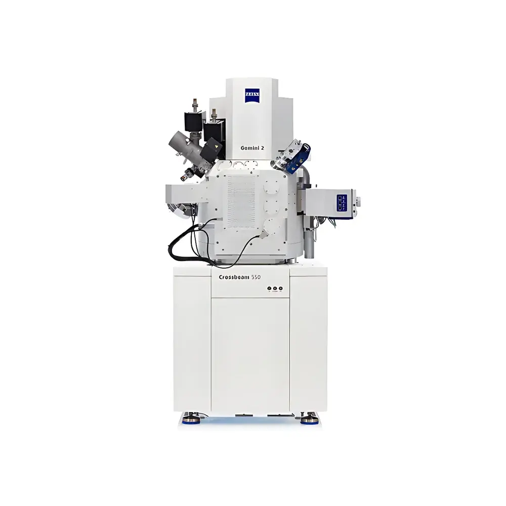
ZEISS Crossbeam 550 FIB-SEM DualBeam Microscope
| Brand | ZEISS |
|---|---|
| Origin | Germany |
| Model | Crossbeam 550 |
| Configuration | Fully Integrated FIB-SEM Platform with Gemini II Electron Optics and High-Current Ga⁺ Focused Ion Beam |
| Maximum Ion Beam Current | 100 nA |
| Resolution (SE, 1 kV, Tandem Decel) | ≤1.4 nm |
| Sample Chamber Options | Standard (18 ports) or Extended (22 ports) |
| X/Y Stage Travel | 100 mm (standard chamber) or 153 mm (extended chamber) |
| Inlens EsB Detector Depth Sensitivity | <3 nm |
| EDS Integration | Full 3D Tomography-Compatible Energy-Dispersive Spectroscopy Module |
| Software Platform | ZEISS Atlas 5 for Automated 3D FIB-SEM Tomography and Correlative Analysis |
| Compliance | Designed for GLP/GMP environments |
Overview
The ZEISS Crossbeam 550 is a high-performance dual-beam focused ion beam–scanning electron microscope (FIB-SEM) engineered for precision nanoscale characterization, site-specific sample preparation, and quantitative 3D structural and compositional analysis. Combining ZEISS’s Gemini II field-emission electron optical system with a high-current gallium-ion FIB column, the Crossbeam 550 delivers sub-nanometer surface imaging resolution and accelerated material removal capabilities in a single integrated platform. Its core architecture leverages Tandem deceleration technology to maintain exceptional secondary electron (SE) contrast and spatial resolution—even at low landing energies (down to 1 kV)—enabling high-fidelity imaging of beam-sensitive, non-conductive, or heterogeneous materials without charge compensation artifacts. The instrument operates on the principle of correlated electron imaging and ion-induced sputtering, allowing real-time feedback between SEM observation and FIB milling, which is essential for iterative 3D tomography, TEM lamella extraction, and cross-sectional metrology in advanced materials science, semiconductor failure analysis, and life sciences.
Key Features
- Gemini II electron column with Tandem decel optics, achieving ≤1.4 nm resolution at 1 kV for surface-sensitive imaging
- High-current Ga⁺ FIB column delivering up to 100 nA beam current for rapid, high-precision milling and trenching
- Inlens EsB detector with <3 nm interaction depth for composition-sensitive, surface-restricted imaging—ideal for thin films and interfacial analysis
- Extended sample chamber option (22 external ports) supporting simultaneous integration of STEM, multi-segment BSE detectors, and localized charge neutralizers
- Automated batch preparation workflows for TEM lamellae, cross-sections, and user-defined geometries via ZEISS Atlas 5 scripting engine
- Fastmill scanning strategy—optimized for angular sputter yield—improves material removal rates by up to 40% compared to conventional raster milling
Sample Compatibility & Compliance
The Crossbeam 550 accommodates a broad range of specimen types—including insulating ceramics, polymers, biological tissues (cryo- or resin-embedded), and semiconductor wafers up to 200 mm (8-inch) diameter—without mandatory conductive coating. Its optional variable-pressure mode (on select configurations) further extends compatibility to hydrated or outgassing samples. All hardware and software modules are designed to meet international laboratory quality standards: the system supports full metadata capture, time-stamped audit logs, and user-access controls aligned with FDA 21 CFR Part 11 when deployed in regulated environments. Instrument calibration, stage positioning, and detector response data are traceable to internal reference standards and compatible with ISO/IEC 17025 documentation frameworks for accredited testing laboratories.
Software & Data Management
ZEISS Atlas 5 serves as the unified control and reconstruction platform for automated 3D FIB-SEM tomography. It enables synchronized acquisition of SE, EsB, and EDS signals during serial sectioning, with voxel-aligned registration of structural and compositional datasets. The software includes built-in drift correction, slice-to-slice alignment algorithms, and GPU-accelerated volume rendering. All raw data—including stage coordinates, beam parameters, detector gain settings, and timestamped acquisition logs—are stored in vendor-neutral HDF5 format, ensuring long-term archival integrity and interoperability with third-party analysis tools (e.g., Avizo, Dragonfly, or Python-based SciPy stacks). Optional modules support automated report generation compliant with ASTM E2967-22 (Standard Guide for 3D Reconstruction from Serial Sectioning).
Applications
- 3D nanotomography of porous media, battery electrodes, and catalyst scaffolds with isotropic voxel resolution
- Site-specific TEM lamella preparation from multilayer metallization stacks (e.g., Ag-Ni-Cu systems), including automated lift-out and thickness monitoring
- Failure analysis in advanced nodes: trenching, cross-sectioning, and EDS mapping of Cu diffusion barriers or gate oxide defects
- Correlative STEM-EDS analysis of grain boundary segregation in stainless steels (e.g., Cr-rich carbides in X2CrNi18-10 heat-affected zones)
- Quantitative microstructure-property correlation studies in additively manufactured alloys and ceramic composites
FAQ
What distinguishes the Crossbeam 550 from the Crossbeam 340?
The Crossbeam 550 integrates the Gemini II electron column with enhanced Tandem decel performance, higher FIB current capability (up to 100 nA), extended chamber port count (22 vs. 18), and larger stage travel (153 mm in extended configuration). It also features native support for Atlas 5’s full 3D EDS tomography pipeline.
Can the Crossbeam 550 perform in situ experiments?
Yes—its modular chamber design allows integration of heating, cooling, or mechanical biasing stages. Optional differential pumping and pressure control enable limited in situ gas or vapor exposure during imaging/milling.
Is EDS quantification supported during 3D tomography?
Yes—Atlas 5 synchronizes EDS acquisition with each FIB slice, enabling voxel-wise elemental distribution mapping. Quantitative analysis requires standard-based calibration and matrix correction routines compatible with standard EDS software packages.
How does Fastmill improve milling efficiency?
Fastmill dynamically adjusts beam incidence angle and dwell time based on local topography and material sputter yield models, reducing redundant passes and increasing volumetric removal rate—particularly effective for silicon, metals, and hard ceramics.
What level of automation is available for TEM sample preparation?
Atlas 5 supports fully scripted workflows for multi-lamella extraction—including fiducial placement, rough milling, final thinning, and cleaning steps—with real-time SE feedback and endpoint detection via electron transparency monitoring.


